
Launched in April 2008, the TSMC Open Innovation Platform initiative is a collaborative strategy aimed at breaking the bottlenecks of semiconductor design enablement in order to promote growth for the industry as a whole. The TSMC iPDK Debate: Lets Play Monopoly! blog I did provides more technical detail.
While Wafer count is climbing, an estimated 20M in 2009 to 30M in 2013, semiconductor design enablement (includes Electronic Design Automation-EDA, Semiconductor Intellectual Property-IP, and Design Services-DS) will continue to stagnate and consolidate.

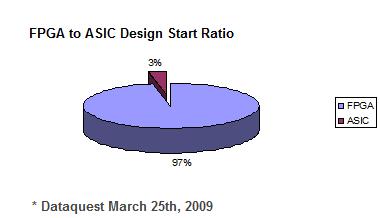
The main reason for the disjointed wafer count increase and design enablement revenue stalling is FPGAs. As programmable devices advance in speed and density, medium-to-small volume projects and emerging technology companies will continue to leverage the low barrier to entry of FPGAs. Wafer count climbs from FPGA vendors such as Xilinx, Altera, and Actel, while ASIC design starts decline.
Other reasons for the ASIC design start decline include:
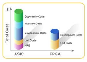
- High cost, it takes $50-70M to get an ASIC to market.
- Increased SOC design density and complexity, the chips are bigger so there are less of them and require many more resources to complete.
- High mortality rate, an estimated 50% of the ASIC design starts do not make it into production.
- Less ASIC design starts equals less design experience, less design experience equals higher ASIC mortality rate.
The TSMC Open Innovation Platform promotes timeliness-driven innovation amongst the semiconductor design community, its ecosystem partners and TSMC’s IP, design implementation and DFM capabilities, process technology and backend services. The Open Innovation Platform™ includes a set of ecosystem interfaces and collaborative components initiated and supported by TSMC that efficiently empowers innovation throughout the supply chain and enables the creation and sharing of newly created revenue and profitability. TSMC’s AAA initiative is a critical part of the Open Innovation Platform™, providing the accuracy and quality required by ecosystem interfaces and collaborative components.

The financial goal of OIP is obvious, to reduce waste in the semiconductor design enablement supply chain. People in this industry are accustomed to waste, business as usual, so this is a significant challenge! Jack Harding of eSilicon estimates a 20% waste due to inefficiencies and lack of experience. I say it is closer to 30% if you include the ASIC mortality rate. 20-30% of $50-70M is a significant amount, especially if you are asking a VC for it.
The TSMC OIP targets include the following areas of inefficiencies:
- PDKs, the iPDK standard is innovation driven versus format driven, which reduces foundry and customer support costs.
- EDA Reference Flows and tool qualification, verified design sign-off flows reduce both costs and customer learning curves.
- TSMC IP portal, documenting silicon proven IP from both TSMC and commercial IP vendors such as Virage Logic. Cross distribution deals are also possible.
- TSMC collaborated services, such as Tela Innovations Power and Area Trim.


The bottom line is that to increase ASIC design starts we must decrease the barrier to entry, we must reduce risk, we must all focus on success based business models:
- TSMC is certainly success based with wafer pricing but must look at reducing NRE (mask costs) which are in the millions of dollars.
- IP companies are success based capable with foundry sponsored IP (free to customers), and royalty based IP, but there are still significant up-front licensing fees for leading edge products.
- Design Services (eSilicon) are definitely success based with per chip pricing for working silicon.
- EDA is still in the dark ages with yearly subscriptions or all-you-can eat product dump pricing where you pay whether you use it or not, whether you are successful or not.
This was the second OIP conference, it was stocked with executives from TSMC and the design enablement food chain. The keynotes, panels, and discussions were highly interactive, the format and content is exactly what our industry needs to scale and move forward in a profitable manner.
Share this post via:


