

Launched in April 2008, the TSMC OIP initiative is a collaborative strategy aimed at breaking down the barriers of semiconductor design enablement in order to reduce waste and increase the profitability of the industry as a whole.
The TSMC Open Innovation Platform promotes timeliness-driven innovation amongst the semiconductor design community, its ecosystem partners and TSMC’s IP, design implementation and DFM capabilities, process technology and backend services. The Open Innovation Platform™ includes a set of ecosystem interfaces and collaborative components initiated and supported by TSMC that efficiently empowers innovation throughout the supply chain and enables the creation and sharing of newly created revenue and profitability.

The TSMC OIP targets include the following areas of inefficiencies:
[LIST=1]
- PDKs: the iPDK standard is innovation driven versus format driven.
- EDA Reference Flows and tool qualification, verified design sign-off flows.
- TSMC IP portal: documenting silicon proven IP from both TSMC and commercial IP vendors such as Virage Logic.
- TSMC collaborative services.The annual TSMC OIP conferences are stocked with top semiconductor, EDA, and IP executives from around the world. The keynotes, panels, and discussions are highly interactive, the format and content is truly collaborative and exactly what our industry needs to scale and move forward in a profitable manner.
A new entry to this format is the Cadence Open Integration Platform launched inside the infamous EDA360 Manifesto. As they say, identify theft is the sincerest form of flattery:
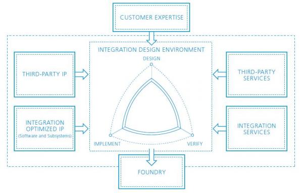
Cadence Design Systems, Inc. (NASDAQ: CDNS), the global leader in EDA360, today announced the Cadence Open Integration Platform, a platform that significantly reduces SoC development costs, improves quality and accelerates production schedules. A key pillar in support of its EDA360 vision for next-generation application-driven development, the Cadence Open Integration Platform comprises integration-optimized IP from the company and its ecosystem participants…
The goal of both OIP’s is obvious, to reduce waste within the semiconductor design and manufacture process. People in this industry are accustomed to waste, business as usual, so this is a significant challenge! A former co-worker, Jack Harding CEO of eSilicon, estimates a 20% SoC design waste due to inefficiencies including lack of process node design experience. I say it is closer to 30% if you include the SoC mortality rate. 20-30% of the $50-100M SoC “realization” cost is a significant amount, especially if you are borrowing the money from a VC.
The result of my expert analysis in the case of TSMC OIP versus CDNS OPI is based on the definition of the word:
col·lab·o·ra·tion–noun1. the act or process of collaborating.
2. a product resulting from collaboration: This dictionary is a collaboration of many minds.
TSMC follows the academic definition as the key to the fabless semiconductor design and manufacturing business is collaboration. Transforming a closed (IDM) design and manufacture process into a truly open semiconductor foundry business is an amazing thing and TSMC clearly has earned the title “Global Leader in Fabless Semiconductor Design and Manufacture”.
CDNS brings a new definition to the word collaboration by alienating (opposite of collaborating) key partners in the ecosystem:[LIST=1]
- Process pioneering foundries and semiconductor manufacturing equipment companies (EDA360 says new process nodes are scary so you should stay at older nodes as long as possible.)
- EDA and IP Bretheren. (Cadence is the self appointed “Global Leader of EDA360”, which is nothing more than the repackaging of existing technology with a big public relations bow on it.)
- Customers. ( Is this not deja vu of the arrogant behavior during the Cadence Fister/Intel era? Ditching DAC, cutting partner programs, etc…)
In the hands of the EDA Consortium (EDAC), EDA360 would be a brilliant blueprint for the EDA industry and could easily replace “Where Electronics Begins”. Unfortunately, in the hands of Cadence it will not. My bet is that CDNS EDA360 will in fact be John Bruggeman’s Waterloo and CDNS OIP will be renamed or will die a silent death. Just my opinion of course, but I am the Global Leader of Independent Semiconductor Bloggers.


