


This blog posting is sponsored by EVA airlines, as I’m in the EVA executive lounge eating free food (I blog for food). “Fly EVA, the lesser of evils for Taiwan air travel!” EVA Air has a perfect safety record in 9 years of operation, China Air on the other hand has the worst safety record in the industry!
This blog was inspired by one of the longest, most spirited discussions I have read on a LinkedIn semiconductor group. A question posted on the Semiconductor Professionals Group five months ago, starting with a simple question, “Any status of 450mm? Who will be adopting first?”. It is followed by 160+ comments from semiconductor experts around the world.
TSMC, Intel, Toshiba, and Samsung all support the transition to 450mm citing both important technological advancements as well as significant capacity increases to meet the needs of future smartphone users around the world. One 450mm wafer should yield more than twice as much compared to today’s 300mm, and well over four times the number from yesterday’s 200mm.

Unfortunately, the semiconductor equipment manufacturers, the enablers of 450mm wafers, lost more than $1B and released 30%-40% of their workforces in 2009. Once scheduled for a 2012 launch, the transition to 450mm wafers has been delayed due to the financial meltdown. But with the current semiconductor industry upswing with foundries like TSMC and UMC operating at maximum capacity, the 450mm debate continues.
The debate about 450mm really boils down to: Will 450mm increase total capacity while reducing manufacturing costs? And is 450mm the best way to accomplish this?
According to Thomas Sonderman, Vice President of manufacturing systems and technology at GlobalFoundries:
“The rush to 450mm suggests a lack of ideas for improving fab productivity. At GlobalFoundries, we see a tremendous amount of headroom left in the 300mm process. We are tapping our expertise in lean manufacturing to extend the lifecycle of the industry’s current 300mm investments, and we are investing more than $4 billion in a new, state-of-the-art 300mm fab in upstate New York because we are confident in our ability to get the most out of this technology generation.”
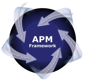
The key to GLOBALFOUNDRIES “lean manufacturing” is a model based on highly automated decision-making called Automated Precision Manufacturing (APM). APM was a key technology that enabled AMD to compete as an IDM, which GlobalFoundries is now offering to a broader base of customers as a foundry.
According to Jack Sun, Vice President, Research and Development and Chief Technology Officer at TSMC:
“A move to 450mm is important for cost reduction and I believe it’s going to happen. The device manufacturers and governments all have to pitch in and contribute to the effort. People will find a way to invest so that we can deliver 450mm. Before the credit crunch, the target was 2012. It has moved out a couple of years, it has pushed out to the middle of this decade.”
In the early days of semiconductor, the device manufacturers themselves produced the required tools and equipment. That could easily come full circle with 450mm. With a limited amount of potential customers and under staffed and under funded semiconductor manufacturing equipment companies, Intel, Samsung, TSMC, and Toshiba, may be forced to develop 450mm manufacturing tools and machinery. TSMC already has 450nm enabling equipment in-house for R&D, alpha, and beta testing. Intel, Toshiba and Samsung may have internal 450mm development activities as well.
According to Daniel Nenni, famed semiconductor blogger:
“450mm manufacturing capabilities will separate the men from the boys. If Samsung (Korea) is the only memory manufacture with 450mm capabilities, Micron (USA), Toshiba and Elpida (Japan), and Taiwan Memory, will be dog food. If TSMC (Taiwan) is the only foundry with 450mm manufacturing capabilities, TSMC will be the Great Dane of the semiconductor world!”

lang: en_US
Share this post via:


