
On July 4, 2012, the European Organization for Nuclear Research, or CERN, announced that the ATLAS and CMS experiments had each observed a new particle, which is consistent with the Higgs boson predicted by the Standard Model of particle physics. The Compact Muon Solenoid (CMS) is a general-purpose detector with a broad physics program that includes the Higgs boson. The CMS experiment is one of the largest international scientific collaborations in history, involving 4,300 particle physicists, engineers, technicians, students and support staff from 182 institutes in 42 countries.
Another prominent feature of the CMS experiment has been the extensive use of semiconductor devices—around 1 million chips in which nearly 700,000 units are ASICs—that range from pixel detectors to Si sensors to calorimeter chips. The ASIC design work is imperative in the high energy physics (HEP) community experiments because commercial off-the-shelf (COTS) components don’t meet the high-radiation, high-magnetic-field and low-power requirements.

A CMS experiment consumes nearly 1 million chips
The large-scale ASIC development is a giant challenge in its own right. However, the collaborative nature of work carried out at CERN brings a new conundrum that goes beyond the labyrinth of technical challenges generally associated with integrated circuit (IC) design work. There are around 30 engineers in CERN’s microelectronics team, and they are collaborating with 70 to 120 chip designers from 20 to 30 universities and research institutes. So, typically, design teams involved in the CERN projects are dispersed geographically as well as institutionally.
And here comes the design conundrum for CERN: The chip industry is facing a number of challenges in dealing with traditional ad hoc ASIC design methodologies. And CERN’s situation, where it’s hard to get all the stakeholders in an ASIC design project in one room, further exacerbates design challenges. In addition, the sheer scale of the number of ASICs used for such a scientific undertaking means that huge data volumes are circulating in a project.
Traditional ASIC Design Challenges
Wojciech Bialas is an IC design engineer at CERN’s microelectronics group. He shared his views on ASIC design flow problems that chip designers face at CERN at the CDN Live EMEA in Munich, Germany at the end of April. He also explained the solution that allowed ASIC designers at all sites to have access to all design data as well as changes in real-time: a multi-site design collaboration scheme. A quick recap of the design problems first.
In a traditional ASIC design flow, chip designers have scratch libraries for development, and they share master libraries that contain the finished cells. Chip designers create or edit cells in their personal scratch libraries, and then they verify them using the master libraries. ASIC designers verify the design by using the limited remote site collaboration available through either rsync or ftp,which is relatively time consuming. Access control is mostly based on trust, and if there is new design release, it’s archived in the master library.
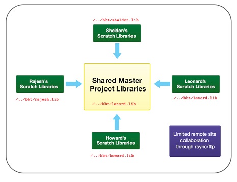
Ad hoc ASIC methodologies offer no traceability of design changes
However, traditional design flow is quickly running out of steam for collaborative ASIC design work. For a start, design changes are usually tracked through e-mails and meetings. Chip designers can accidentally overwrite each other’s changes. Moreover, it’s hard for them to know when changes are lost, so they end up losing track of what different versions mean.
As a result, libraries become cluttered with unwanted cells and design versions. The notion that any user can make changes in libraries at any time also creates doubts about the quality of simulation and verification work. All this leads to a high risk of miscommunication and delayed turnaround for design fixes.
Design Data Management
EDA toolmakers like Cadence Designs Systems have started integrating an API layer for third-party data management solutions. That allows all design data and revisions to be managed through a project repository like SOS from ClioSoft Inc. SOS is a design data and IP management platform that is integrated with leading design flow tools such as Cadence’s Virtuoso, Mentor’s Pyxis, Keysight’s ADS and both Synopsys Custom Designer and Synopsys Laker.
The SOS project repository allows each user to have a separate and isolated work area, and each work area has a read-only linked copy of the project libraries. That allows ASIC designers to check out a writable copy of cell before editing. They can edit existing cells or create new cells in their work area. When a user changes the history of an object, the SOS data management tool automatically updates the entire project. Given the sensitive nature of the data, SOS provides administrative controls to manage design access.
SOS provides tracking and accountability of design changes
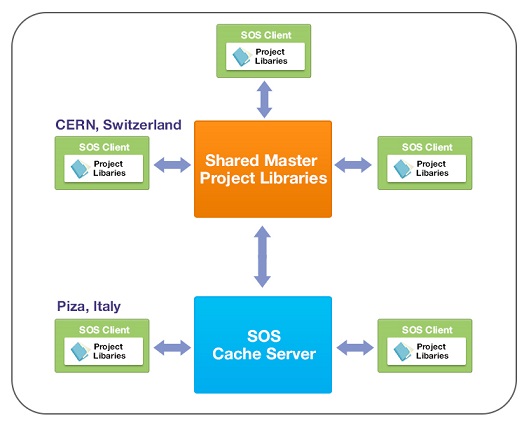
The primary SOS server located at the CERN headquarters in Switzerland manages the project repository that contains the entire project data and revisions. The distributed architecture of the SOS tool, however, permits different repositories to be set up at different locations as needed. At each remote site, cache servers are set up and automatically update with changes. In other words, ASIC designers at all sites have access to design data and changes in real-time. Designers without access to cache server infrastructure are allowed CERN computing accounts with encryption tunnels for appropriate access control.
CERN’s Bialas acknowledged that the use of SOS data management frees CERN engineers from the need for periodic syncs and artificial partitioning of ASIC designs. Moreover, it allows design managers to accomplish an optimum use of resource bandwidth among different sites.
Bialas also shared his views on the Visual Design Diff software, another ClioSoft product that displays design differences in schematics, layout and RTL. It’s particularly useful in ECO flows to track the changes made between different versions of the same design on which different design engineers are working. Bialas noted that the use of Visual Diff allows ASIC designers to quickly see the difference between the revisions. Moreover, users can take snapshots to record new configurations, and these snapshots can be recreated at any time in the design cycle.
As the 100+ designers in the CERN project discovered, ClioSoft allows companies and institutions to use the best talent, worldwide, on every project. Collaboration in real time and worldwide revision control enable exploration in new areas of growth.
Majeed Ahmad is the former Editor-in-Chief of EE Times Asia and is the author of six books about the electronics industry.
Also Read
ClioSoft Celebrates 2014 with 30% Revenue Growth!
Secret Sauce for Successful Mixed-signal SoCs
DNA Sequencing Eyes SoCs for Stability and Scale
Share this post via:


Comments
There are no comments yet.
You must register or log in to view/post comments.