

My vote for most compelling technology at #47DAC is 3D technology. No, I don’t mean Hollywood-style 3D, I’m talking about vertical stacked-die system on chip design. This design approach basically means putting different parts of the system on different silicon substrates, so you can use the right technology for each part, and then stack them vertically.

3D technology promises to reduce cost and improve performance. By putting different parts of the system on a slice of silicon from an optimized process, you don’t have to do things like shoe-horn mixed signal parts into advanced process nodes, which is very expensive and doesn’t really work that well for mixed signal anyway. Because the interconnect between the silicon slices is very short (due to the stacking), wiring delays are minimized and performance should be very good.
There was a lot of talk about 3D at #47DAC last week. Many EDA vendors are jumping on the bandwagon and announcing plans to support it. A session that stands out as one of the more realistic and informative events on the topic was put on by Atrenta, IMEC, AutoESL, and Qualcomm. Front-end design issues were discussed and a front-end flow was demonstrated.
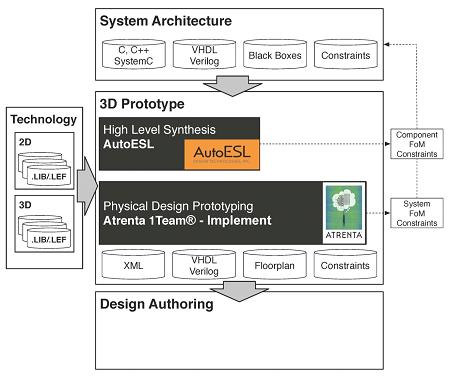
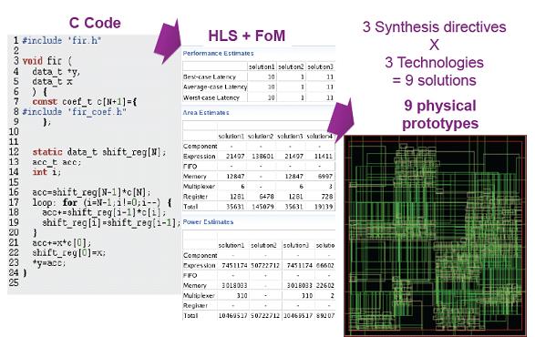
Besides seeing real, working software and not just PowerPoint, this session got my attention because it pointed out how different 3D design will be. One of the main challenges with this technology is choices, too many choices. The demo drove this point home by running different options for a 3D design through a high-level synthesis and virtual prototyping flow. AutoESL provided the high-level synthesis and Atrenta provided the virtual prototyping. If a designer would like to consider 3 different micro-architectures (like loop-unrolling, pipelining or standard) and three different technology choices (like 90, 65 or 40nm), then there are nine possible ways to implement this part of the 3D design. But which one should you choose?
The demo showed how to implement the three different micro-architectures and three different technology nodes by using various synthesis directives for the AutoESL tool. You start with C code and end up with RTL during this part. The Atrenta prototyping tool then read in the nine options and created a physical virtual prototype for all of them, complete with routing congestion and timing data. If you look at the options this way, it starts to become clear which one to choose.
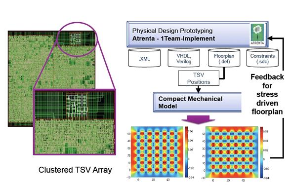
I can’t imagine having the time to go through a complete back-end flow to figure this out, so the front-end planning part seems pretty important for 3D design. Another challenge with 3D appears to be thermal and stress modeling. Stacking dies like this creates all kinds of stress and heat problems. IMEC showed an interface between Atrenta’s prototyping tool and compact thermal and stress models they developed. Very impressive!
By the time this session was over, my brain was hurting from all the degrees of freedom implied by 3D. It will be interesting to watch as 3D becomes real over the next couple of years. We’ll see who wins, but for now, IMEC, Qualcomm, Atrenta, and AutoESL seem to have a jump on some of the hard problems. Please let me know your thoughts in the comment section, I can assure you, 3D EDA vendors will be reading them.


Real men have fabs!