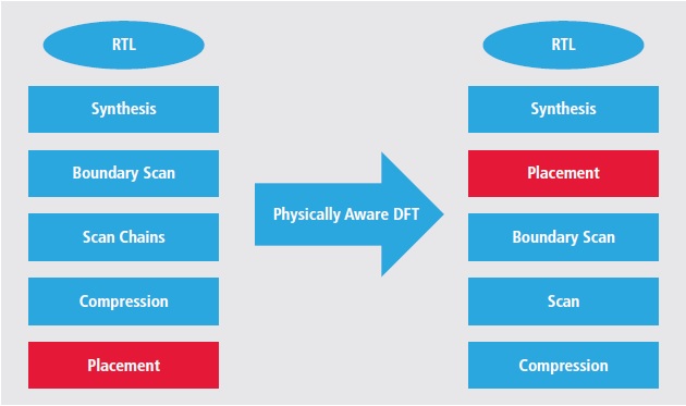
Introducing on-chip test circuitry has become a necessary criteria for an ASIC’s post manufacture testability. The test circuitry is usually referred as DFT (Design-for-Test) circuit. A typical methodology for introducing DFT circuit in a design is to replace usual flip-flops with special types of flip-flops called ‘scan flip-flops’ that contain logic targeted for improving testability. Scan chains are formed by connecting scan flip-flops serially that allow Automatic Test Pattern Generation (ATPG) tools to control and observe the sequential state of the design and to generate test patterns to achieve the highest fault coverage. Further, extra circuitry can be added to compress test data volume and optimize test time. Also, several self-testing logics, such as logic built-in self-test (LBIST) and memory built-in self-test (MBIST) can be added on a chip.Clearly, the DFT circuits are a must for testability, reliability and robustness of designs. However, they introduce overheads in terms of area and wiring which can increase power consumption and decrease performance of a design substantially. Also, accommodating clock domain crossing (CDC), clock-edge mixing, and voltage domain crossing in an SoC (which can have multiple modes of operations) needs extra hardware such as lock-up latch and voltage level shifter. This extra hardware introduces additional wiring along the scan path resulting into excessive wiring congestion. So, what’s the alternative in such a dilemmatic situation? We truly do not have a choice. We need to use the DFT circuitry. What if we have the best of both worlds? Here is a smart methodology where the overall design is optimized for best PPA (Power, Performance and Area). The idea revolves around doing design placement before test circuit insertion. Traditionally, placement is the last stage in the design flow when scan chain re-ordering is done to shorten long wires in the scan-paths. Naturally, this approach is limited in the sense that placement cannot be changed to a large extent. The break-point logic on the scan-path that involves lock-up latches, clock crossings, etc. cannot be affected to re-order flip-flops. Hence only feasible long wires can be re-routed. In a new approach at Cadence, a scan-mapped netlist is placed just after synthesis, before inserting DFT. Then, based on the placement, scan flip-flops are assigned to scan chains. Further, scan chain re-ordering is done as a final step.Cadence implemented this new methodology on a real wireless communication chip by using its ‘Encounter Digital Implementation System’ and ‘Encounter RTL Compiler Advanced Physical’ that provided an impressive gain of ~16% in scan-chain wire length reduction compared to traditional methodology. The net result in PPA optimization was ~42% saving in total negative slack in timing, ~5% saving in power and ~2% saving in area. Actual detailed data and the detailed steps applied in the flow by using these tools can be found in a whitepaperfreely available at Cadence website.The whitepaper also describes about how Encounter RTL Compiler leverages I/O pad placement information to optimally order the boundary-scan cells in the boundary-scan shift register. IEEE 1149.1 boundary-scan testing is essential for board-level interconnect testing. Here, boundary-scan cells are inserted between I/O pads and the system logic. The boundary-scan cells are serially connected and provide controllability and observability to board-level interconnects. Their ordering is also important to minimize long crossovers along functional paths.The Cadence’s physically aware DFT methodology is proven to prevent wiring congestion due to DFT insertions, thus providing significant improvements in power, performance and area optimizations of a design.


Comments
There are no comments yet.
You must register or log in to view/post comments.