

Power grids all over the world are already overloaded even without the slew of new electronic gadgets and cars coming out this year. At ISSCC, Dr. Jack Sun, TSMC Vice President of R&D and Chief Technology Officer made the comparison of a human brain to the closest thing available in silicon, a graphical processing unit (GPU).

Dr. Jack Sun is talking about the NVIDIA GPU, I believe, as it is the largest 40nm die to come out of TSMC. The human brain has more than 100 billion neurocells (cells of the nervous systems). 100 billion neurocells consume 20 watts of power versus 200 watts for an equivalent amount of transistors in silicon. The bottom line is that semiconductor technology is severely power constrained and he suggests that we must learn from nature, we must look at technology from the bottom up.
“New transistor designs are part of the answer,” said Dr. Jack Sun. Options include a design called FinFET, which uses multiple gates on each transistor, and another design called the junctionless transistor. “Researchers have made great progress with FinFET, and TSMC hopes it can be used for the next generation of CMOS — the industry’s standard silicon manufacturing process,” Sun said.
According to Wikipedia:
The term FinFET was coined by UniversityofCalifornia,Berkeleyresearchers (Profs. Chenming Hu, Tsu-Jae King-Liu and Jeffrey Bokor) to describe a nonplanar, double-gate transistor built on an SOI substrate,[SUP][5][/SUP]based on the earlier DELTA (single-gate) transistor design.[SUP][6][/SUP]The distinguishing characteristic of the FinFET is that the conducting channel is wrapped by a thin silicon “fin”, which forms the gate of the device. The thickness of the fin (measured in the direction from source to drain) determines the effective channel length of the device.

So now you know as much about a FinFET as I do.
After the panel I had a conversation with Dr. Sun about power and looking at it top down from the system level. TSMC is already actively working with ESL and RTL companies (Atrenta) to do just that. Designers can optimize for power consumption and efficiency early in the design cycle at the register transfer level (RTL). Using commercially available tools, information about power consumption is available at RTL and can provide guidance where power can be reduced, in addition to detecting and automatically fixing key power management issues. Finding and/or fixing these types of problems later in the design cycle, during simulation or verification, can be costly and increase the overall risk of your design project finishing on time and within predetermined specifications.
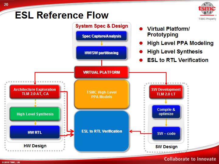
TSMC’s current Reference Flow 11.0 was the first generation to host an ESL/RTL based design methodology. It includes virtual platform prototyping built on TSMC’s proprietary performance, power, and area (PPA) model that evaluates PPA impact on different system architectures. The ESL design flow also supports high level synthesis (HLS) and ESL-to-RTL verification. TSMC also expanded its IP Alliance to include RTL based (soft) IP with Atrenta and others. Atrenta is known for the SpyGlass product which is the defacto standard for RTL linting (analysis). If you do a little digging on the Atrenta site you will find the Atrenta GuideWare page for more detailed information.
But of course TSMC can always do more to save power and they will.
Share this post via:


Comments
0 Replies to “Semiconductor Power Crisis and TSMC!”
You must register or log in to view/post comments.