

Since power has become a critical factor in semiconductor chip design, the stress is towards decreasing supply voltage to reduce power consumption. However, the threshold voltage to switch devices cannot go down beyond a certain limit and these results in an extremely narrow margin for noise between the two. And that gets further challenged from increased variations in switching current and parasitics due to growing density and complexity of design in an SoC. Hence it becomes essential to analyze and optimize the complete power delivery network (PDN) of the system including the chip and package together to ensure reliable and stable voltage levels at all connection points of transistors. Amid minimum number of layers for package implementation and increased number of power domains in low power design arena, the package design plays a very important role (optimizing package impedance) in system design and must be considered together with the chip.
ANSYSRedHawk-CPA provides a comprehensive, accurate, fast and automated solution for any large system’s power integrity which accounts for L(di/dt) effects due to package inductance and decaps in its on-chip simulation. Its 3D FEM (finite element method) model based engine enables accurate extraction (high resolution per-bump distributed RLCK parasitics) of package layout for use in RedHawk simulation. The distributed modeling, which provides much finer pad voltage distribution than lumped model, enables accurate identification of weak pad placements that can lead to high dynamic voltage drop for instances in that region. RedHawk-CPA generates a broadband Spice netlist with ground parasitics and uses RedHawk to measure ground bounce separately, thus enabling net-by-net review of voltage drop and optimization of net geometries. Similarly, the package decaps enable instance-by-instance review of voltage drop, also taking into account the package decoupling, thus enabling optimization of package decap configuration.
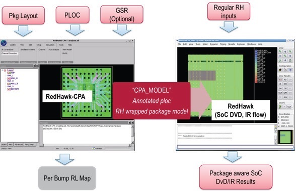
The package layout (in any common format such as MCM, SIP or ODB++) can be directly imported into RedHawk-CPA and after its setup, the PLOC (bump location file) can be imported which is followed by automatic connections between package pins on the layout and bump locations on the chip without needing any designer to manually write connections in a text file in PLOC format, thus improving usability and productivity to a large extent. Of course, through an easy-to-use GUI, there is provision for a designer to override the automatic connections and do it manually as desired for particular connections. The voltage sources are assigned and the package model is generated that can be used seamlessly in RedHawk with GSR keyword ‘CPA_MODEL’, thus eliminating all designer written files including Spice wrapper with RLCK values of package instantiated under REDHAWK_PKG sub-circuit. RedHawk-CPA also allows designers to quickly perform static IR drop and AC hotspot analyses of the package layout following the RedHawk static and dynamic analyses respectively.
The high performance and capacity package extraction engine can easily handle large packages with quick turnaround time, allowing designers to quickly iterate over different chip-package designs and make important decisions such as bump placement early in the design cycle.
The RedHawk-CPA provides a very comprehensive report of design information, component Spice models, channel information, simulation control setup and results with maps and histograms that allow designers to easily review and visualize results.
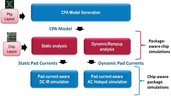
The chip-package co-analysis provides simulations in both ways – package-aware chip simulation and chip-aware package simulation. The package DC IR simulation provides package static IR map which can be reviewed for current density violations on the PG nets of the package layout. The 3D FEM engine in RedHawk-CPA also allows designers to review AC hotspots on a given package layout based on the frequency content in the pad currents from RedHawk transient simulation. It allows a designer to review voltage/current maps/waveforms over the package layout/nodes over a desired frequency range. Near and far field EMI computations are also supported.
It’s a unique solution for chip-package co-design and analysis which is necessary to provide stable power delivery, reduce power consumption and maintain high reliability for today’s SoCs with high PPA factors. A further detailed description is provided in a whitepaperat ANSYS website.
I admire ANSYS also scheduling two separate sessions of free webinars where experts will provide practical level details on how to use RedHawk-CPA for chip-package co-analysis through its unified environment to perform DC, transient and AC power integrity analysis using chip and flip-chip package layouts to improve level of accuracy and shorten time to power closure –
Achieve Faster IC Power Closure Using Streamlined Chip-Package Co-Analysis
Tuesday, Sep 23, 2014 – 9:00 AM EDT, 1:00 PM GMT – Register here
Thursday, Sep 25, 2014 – 4:00 PM EDT, 8:00 PM GMT – Register here
These are very useful webinars to gain practical knowledge about system level issues with power and how to perform robust, accurate power integrity analysis and fix issues to design reliable SoCs.
More Articles by Pawan Fangaria…..
Share this post via:


Comments
There are no comments yet.
You must register or log in to view/post comments.