

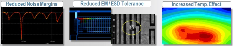
Although semiconductor manufacturing has taken off with FinFET based process technology which provides lucrative payoffs on performance improvement, power reduction and area saving in devices for high density and high performance SoC demand of modern era, apprehensions remain about its reliability due to reduced noise margin, EM and ESD tolerance, and increased heat generation. The increased level of switching due to high density of circuit at higher peak currents and higher grid impedances lead to higher voltage drops, and that combined with reduced supply voltages affects both noise margin and power significantly. The increased voltage drop heightens temperature and thus affects EM reliability of devices as well as interconnects. The FinFET technology also exhibits poor diode protection and that coupled with reduced interconnect reliability can render the chip vulnerable to ESD issues.
So, how to tackle these issues in order to avail the nonpareil advantages of FinFETs? I like Ansys’snew offerings in its RedHawk 2014 platform. My sincere appreciation for Ansys’s effort to proliferate the learning about the real challenges of FinFET technology and how to use RedHawk 2014 to estimate, measure and analyze various parameters to sign-off the semiconductor design at full-chip and package (including 3D stacks) level for power, noise and reliability with silicon correlated accuracy, pico-second resolution and maximum sign-off coverage.
After an overwhelming response to Ansys’s presentation on RedHawk 2014 capabilities to analyze and sign-off FinFET based designs in DAC, they are now unveiling a free webinarfor a larger audience across the world which will provide details about the challenges involved in FinFET based designs and amid those challenges how to address power, noise and reliability sign-off by using RedHawk 2014. The webinar will also provide information about RedHawk certification for 22nm, 16nm and 14nm FinFET processes from multiple foundries.
The new attractions are DMP (Distributed Machine Processing) providing major capacity and performance boost for billion transistor designs including multiple IPs, CPA (Chip-Package Co-Analysis) providing accurate power integrity and reliability analysis including the package impact on die, and temperature-aware EM methodology.
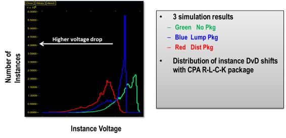
The above image provides a glimpse of package impact analysis on DvD (Dynamic Voltage Drop) with RedHawk-CPA; it considers distributed parasitic network with pin-to-pin mapping.
There are powerful connectivity checks which can determine grid and design weaknesses including power/ground balance, resistance issues, missing vias, static IR, high power density, placement of pads, switches and so on.
The robust reliability checks include power and signal electromigration, chip and system thermal modeling, ESD, clamp placement, cross domain, current density and so on.
The power & noise sign-off includes package-aware chip simulation and chip-aware package simulation with multi-domain power up/down analysis. The vector, vectorless and mixed-excitation analyses are done to improve sign-off coverage along with accuracy. Timing hotspots are also analyzed along with the DvD map.
To know details about these technologies and methodologies, it’s worthwhile attending the webinar. Here is the schedule –
Date: Wednesday, Jun 25[SUP]th[/SUP] 2014
Time: 11:00 AM PDT
Register here to reserve your valuable time and participation in the webinar.

I am excited to hear Calvin Chow, Area Technical Manager at Ansys-Apache, who will provide a great insight into FinFET technology challenges, various tools within the RedHawk 2014 platform and their capabilities to address the reliability of semiconductor designs with FinFETs within the realm of these challenges. Stay tuned to hear more on this.

More Articles by Pawan Fangaria…..
lang: en_US
Share this post via:


Comments
There are no comments yet.
You must register or log in to view/post comments.