“IP Innovation is moving from component level to system level”. This mantra was heard during the conference, from various speakers: during the keynote talk by Ganesh R. from Gartner and presentation “Integration-Optimized IP from Cadence” by Ranga Srinivasan, also during discussion around coffee (or a glass of wine, but this was in the evening).
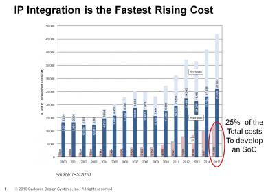
I guess everybody will agree on the principle, somehow it’s like moving from LSI to VLSI 30 or 40 years ago. Cadence’ presentation interest was to clearly state the problem the chip maker involved in SoC design are facing. First, the IP integration costs are the most rising, between Software, Hardware and IP, as it can be seen on Figure 1. In fact, this IP Integration cost has doubled from 2005 to 2010 to reach $5B, and will again doubled to reach $10B in 2014. To make it clear, this is the total cost of ownership for a certain IP, not only the License cost. Within five years (in 2015), it will represent 25% of the total cost to develop a SoC.
Then, it clearly makes sense: first to invest into this fast growing market (like Synopsys is doing for almost 10 years now, and Cadence more recently), second to come with a solution attractive enough to catch more customers. If you dream about coming with the new fantastic CPU core, expecting to get (even) 10% of ARM’ market share, it’s better to give up now! A better starting point would be to look at functions which are common components that are not unique to the design, which you can find in many SoC.
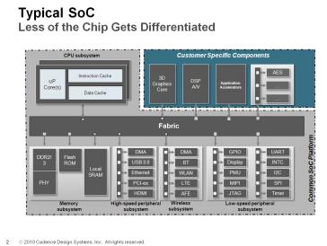
According with another slide presented at IP-SoC, the common functions are: memory subsystem, High speed Interface, Wireless and Low speed Interface subsystems. In term of SoC complexity (gate count) these functions represent the most important part of the chip, when compared with the components which are unique to a SoC, the differentiators which are customer specific.
This is a well known status, and the reason why the IP market is growing (when the ASIC/ASSP design starts are declining) is that reuse is becoming mandatory, when the SoC are getting more and more complexes and the time to market (TTM) tighter. The adoption rate for (internal or external) IP is growing, because it is the only way to keep the design cycle within realistic timeframe (12 to 18 months). If you take the example of the SoC for Set Top Box, a consumer product under a very high TTM pressure, these IC can integrate up to 80 different IP, digital and mixed signal components. In this case, we can imagine that external sourcing has reach a limit in volume of functions externally sourced. Then, what could be the next step? Why not moving up in the food chain, or in the value associated with an IP?
Let’s take as an example one of the High Speed Interface (PCIe, HDMI or USB 3.0 in the above figure). The Interface is made of two H/W components; the PHY and the Controller. To be completely functional, you need to add the S/W components: the design and verification constraints, and the drivers. If you provide all of these, you have moved from a “component IP” provider to an “IP stack” provider. The design team will now integrate the complete Interface function. In fact, this trend is becoming a reality and explains the success of the IP vendors able to provide an integrated solution (PHY plus Controller) like Synopsys for the Interface IP market in general. Or Silicon Image for the HDMI and SATA market, as they can also provide the S/W stack, thanks to their parallel ASSP product lines. So, if this model is successful, why stop at the “IP stack”? Cadence, in the presentation made at IP-SoC, is going further:
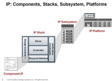
Using the same SoC as an example, the next move would be to propose an “IP Subsystem”, all the High Speed Interface (PCIe, HDMI and so on) integrated together, all the Low Speed Interface integrated together…and so on. The ultimate step being to procure an “IP Platform”, integrating all the common components tied together. If you present it this way, it looks very logical and almost irrefutable.
So, why do I feel not totally convinced?
Is it because you also can introduce differentiation in these so called “common functions”? For example, certain IDM consider that using an internally designed PHY to support the high speed Interface function is one of their differentiators (I could name three of them in the wireless handset segment only). What about the differentiation based on the use of the latest DDRn specification to offer the best memory bandwidth on the market? I am sure we could find many other examples in which part of the SoC differentiation is coming from these common functions… On the other hand, which is important for the vendor will be to find enough customers being satisfied to use this “IP platform”.
But which IP platform? We can guess the need would be to use segment specific platform, if not, within a segment, an application specific platform. In this case, you will move the design completion issue for TTM from the chip maker to the IP platform vendor. This means that the “IP vendor” will have to be better in term of design efficiency (cycle time, first time right, power consumption, timing closure, area) than his customer currently are. It looks to be a drastic change of business model, as the IP vendor is almost becoming an IP integrator. How many of the IP vendors currently on the market (the latest count made on Design&Reuse web site gives 468!) are ready for such a move?
On one hand, I am convinced that the trend for the IP vendors is to move from IP component to IP stack is real, and fit with a market demand. On the other hand, I am not sure that the market is expecting to benefit from an application specific IP platform. This would require a drastic change in term of organization, most of the design team workload moving from the customer to the vendor. It could be attractive for start-up to use this service, as it is already the case with Value Chain Producer (eSilicon, Verisilicon, GUC and more).
What is YOUR opinion? Do you think there will be a limit between “IP component” and “IP platform”, an optimum where the market will stabilize? Will this limit being IP stack or IP subsystem? Or you rather think that the FPGA is the limit: when you provide an application specific IP platform, just add a fast customizable area… and you have (re) created the modern FPGA? Do not hesitate to share if you are a designer or not, working for an IP vendor, a Fabless or an IDM!


The Data Crisis is Unfolding – Are We Ready?