

LSI Corporationstarted in 1980s and I had several encounters with it during my jobs in 1990s; not to forget the LSI chips I used to see in desktops and other electronic systems, and I’m happy to see LSI continuing today with more vigour having leadership position in storage and networking space. It provides highly reliable, high performance and power efficient network processors, communication chips and others for media, connectivity and storage applications. Last week, I was pleased to bump into an on-line webinarpresented jointly by Sudhir K. Sharma of Ansys Corp. and Dr. Cornelia Golovanov of LSI Corp. which made me learn how a system level design methodology used at LSI, involving Ansys Apache tools, leads them to precisely pin point the noise introducing elements in a large SoC including die, package and PCB with significantly fast multi-physics simulation technology and eliminate the same to improve reliability and performance of their chips.
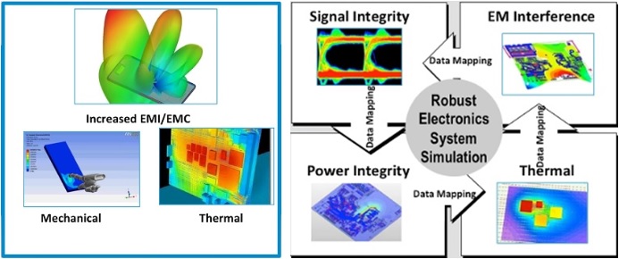
Sudhir talked about the advantages of miniaturization in semiconductor designs with multiple functions working together at low voltages and also introduced about the challenges to maintain their reliability amid high density and complexity leading to crosstalk, thermal and other electrical issues such as reduced noise margin with low operating voltage. It was interesting to note some of the natural phenomena such as mechanical fluid flow and signal attenuation caused by human touch needing a perfect harmony between electrical, thermal and mechanical systems that can handle any kind of variations within specified limits gracefully and predictably.
Let’s look at an interesting case study about which Dr. Cornelia talked at length. This involves system level PDN (power delivery network) analysis including an IO ring sub-system where a bridging happens between power integrity of a PLL as influenced by the large current swings of a DDR PDN and the large signal swings of a DDR signal interface.
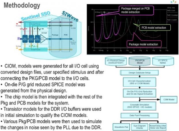
The PG noise in the system can be due to switching activities as well as parallel resonances between PG planes and RLC series resonances and anti-resonances. The switching noise can be due to direct simultaneous switching of digital and analog cells generating transient current spikes and voltage drops. Also, an indirect cause could be due to PG acting as return path of current for switching signal nets; also capacitive coupling between digital and analog supplies. By using Sentinel-SSO, the full chip IO system can be analyzed and contribution of the IO ring switching established. The contribution of DDR signal activity to PLL power integrity can be analyzed and the noise at PLL metal1 pins due to coupling with DDR and chip, package and PCB can be monitored. The Sentinel-SSO enables the simulation of interaction between IO noise and PDN by using transistor models as well as macro models for the IO buffers.
As shown above three different package bonding models were extracted upon soldering the package design onto the PCB. All data bit, address bit and control bit lines as well as the 1.8V and 1.8PLL supplies coupling were accounted.
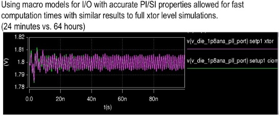
A 100ns simulation with transistor models takes 64 hours whereas the same withmacro models takes just 24 minutes producing similar results.
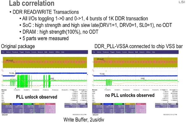
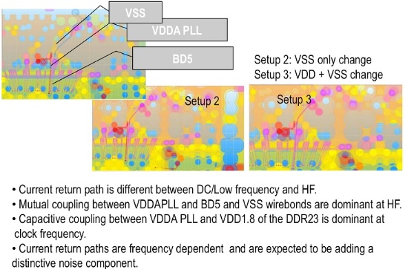
Strong correlation of noise with the lab measurements was observed and LSI found the Sentinel-SSO based methodology to be highly instrumental in intercepting noise due to independently supplied IO cells switching activity severely impacting the dedicated VDDPLL and VSSPLL. Also, the system level workbench encompassing die, package and PCB interconnects exposed the impact of the capacitive and mutual coupling enabled outside the die on the PLL supply. A good correlation between results of pre-layout and post-layout flows was also observed. The methodology provided best selection of solution for PLL supply noise reduction.
A GUI based workbench setup provided by Apache allows quick inclusion and exclusion of on-chip devices. The die can be viewed and analyzed at each layer and via to identify any design weakness. It allows scripting for fast setup of the workbench.
Overall, I found this to be a very novel and robust approach for fast analysis and design of SoCs for high density and complex electronic systems which can meet the kind of PPA (Power, performance and Area) desired in today’s semiconductor community, yet be highly reliable in the long run. A detailed talk can be listened to by logging into the webinar here.

More Articles by Pawan Fangaria…..
lang: en_US
Share this post via:


Comments
0 Replies to “LSI’s Way of Faster & Reliable Electronic System Design”
You must register or log in to view/post comments.