

The semiconductor design sizes, these days, can easily be of the order of several hundred millions of cells, adding into the complexity of verification. Amid ever growing design sizes, it’s a must that the timing verification is done accurately. Normally Static Timing Analysis (STA) is done to check whether all clocks and signals in the circuit at every stage are properly timed. While introducing hierarchy is inevitable in architecting such large semiconductor designs, every level of hierarchy leads to abstraction in timing, thus causing certain amount of loss in accuracy of timing. The EDA vendors are struggling hard to strike a balance between memory usage, run-time and accuracy of timing analysis by using different hierarchical methods of timing analysis; a flat design analysis can provide most accurate results as it runs through each leaf level cell and wires through it, but consumes large amount of memory and needs very long run-time.
Extracted Timing Model (ETM) is a common hierarchical analysis approach which replaces respective blocks by delay and timing constraint arcs to speed-up timing analysis and reduces memory consumption. However, this approach has a major limitation that multiple-constraint modes need to be merged into a single ETM for the top level analysis. Again merging across corners is not possible. Hence, MMMC (Multi-mode Multi-corner) analysis requires extra allocation of time to extract ETMs that comprehensively cover all modes and corners. Moreover advanced on-chip variation (AOCV) requires multiple characterizations (for multiple instantiated blocks) for the same view in analysis. SI-aware ETM, path exception modeling, multiple-master clock modeling for a generated clock, waveform propagation-aware ETM etc. are some of the other limitations and complexities in the ETM approach of timing analysis. Also, this approach is good to work only in a given context. When the context changes (which is typically the case because the context is not known exactly until the end of the design cycle), ETMs must be regenerated.
Another common approach to model a block is Interface Logic Model (ILM), where only the connections from inputs to the first stage of its flip-flops and the connections from the last stage of flip-flops to the outputs remain in the model along with the clock tree driving these flip-flops. All the other internals of the block are wiped out. While this approach can deliver highly accurate results significantly faster at lesser memory consumption, it lacks to comprehend over-the-block routing, constraint mismatches, latch-based designs, and pessimism in arrivals due to timing-window CPPR (Common Path Pessimism Removal). Also, too many ILMs to cover all modes and corners for each timing analysis view would require huge data storage and management.
In order to overcome the issues of ILM and ETM methods, concurrent analysis of hierarchical blocks (where design partitions are timed independently and dependencies between them are resolved by asserting constraints and synchronizing other data at the block boundaries) with an aim at converging iteratively by asserting new constraints at each iteration is attempted. However, this approach also has a set of limitations.
I was very impressed with Cadence’sTempus Timing Signoff Solution which provides full flat timing analysis (naturally most accurate) and uses massive distributed processing to improve and control run-time and capacity. To my pleasant surprise, in order to make the solution more powerful for full chip analysis, Cadence has introduced a new concept, called Scope-based Analysis into its Tempus Solution.
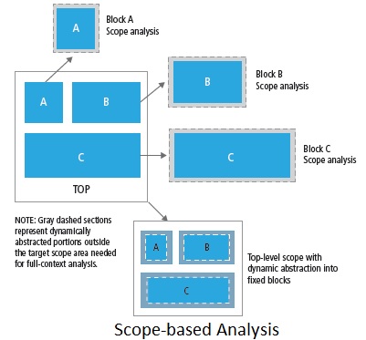
In this approach, only those portions of the design that a user wants to analyze (due to change) are dynamically abstracted with full-chip level context. The user defines the change space at the level of granularity equal to physical/logical block boundaries. Once the blocks or top-level scope is provided to the Tempus solution, dynamic abstraction of the design is done under the hood. Analysis of the resulting design is done in significantly lesser run-time and memory footprint.
This approach is consistent with flat timing analysis providing several major benefits at the user as well as design level. The tool keeps operating with the same user scripts and constraints that were used for flat timing analysis without any change in the use model of timing analysis. The reports produced are also consistent in format and content with that of flat timing analysis, thus saving the user from unnecessary debugging for any deviation. The added value of this approach is 2-3 times faster analysis at significantly less peak memory than a full flat analysis. Also each scope-based analysis can be run in parallel, a key strategy of Tempus Solution. The approach is fully compatible with MMMC analysis without requiring any change in the user-script set up for defining constraints and analysis views.
Since flat-level timing analysis is necessary to achieve accuracy in timing, Tempus Timing Signoff Solution along with its innovative Scope-based Analysis approach to accurately and efficiently analyze portions of the design affected by the design change, provides the ultimate experience in full chip timing analysis of large semiconductor designs of the order of hundreds of millions of cells. One can read a whitepaper describing in detail about this and other methods of hierarchical timing analysis.
More Articles by Pawan Fangaria…..
lang: en_US
Share this post via:


Comments
There are no comments yet.
You must register or log in to view/post comments.