

I spend about an hour a day reading blogs from EDA companies, foundries, independent bloggers and of course, SemiWiki. Richard Goering at Cadence assembled a top 10 list of the most popular blogs posted on their site in 2013, revealing that engineers were most interested in: FinFETs, 20nm and smaller nodes, memory technology and PCB design.

Richard Goering, Cadence
The community bloggers at Cadence wrote some 375 articles this year, that’s over 7 new blogs per week, so expect lots of fresh material and it’s all organized by categories so that you can quickly find what interests you most.
The Top 10
1. TSMC 2013 Symposium: Progress in 20nm, 16nm FinFET, and 3D-IC Technologies
From April 9th, presentations about 20nm planar, 16nm FinFET, and Chip-on-Wafer-on-Substrate (CoWoS) technologies. Also a sneak peek at 10nm FinFETs and 3D die stacking.
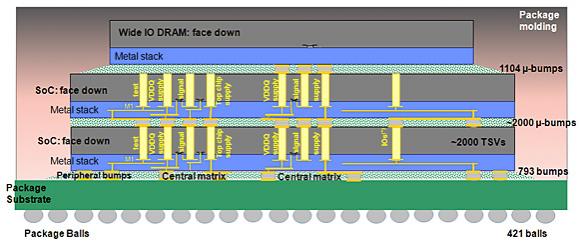
2. Wide I/O 2, Hybrid Memory Cube (HMC)—Memory Models Advance 3D-IC Standards
MemCon on August 6, Wide I/O 2 and the Hybrid Memory Cube (HMC).
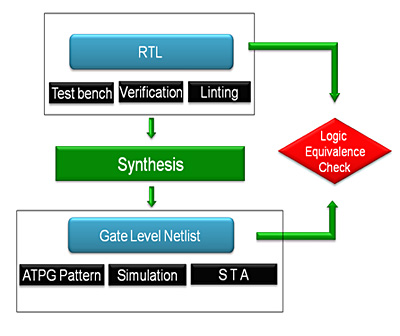
3. Functional Verification Survey—Why Gate-Level Simulation is Increasing
Gate-level simulation is still used to verify DFT inserted gates, timing and x-state detection.
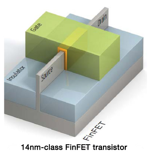
4. BSIM-CMG FinFET Model—How Academia and Industry Empowered the Next Transistor
Collaboration between U.C. Berkeley and industry have created a new model for FinFET devices called the BSIM-CMG model.
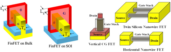
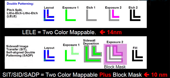
5. 10nm and 14nm FinFETs Pose Challenges—But Collaboration Brings Solutions
Double patterning is still required for 10nm and 14nm design of FinFETs.
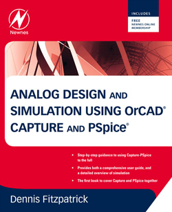
6. New Book: Analog Design and Simulation Using OrCAD Capture and PSpice
Author Dennis Fitzpatrick has written a new book showing how to use schematic capture and circuit simulation for analog designers.
7. MemCon Samsung Keynote: New DRAM and Flash Memory Architectures are Needed
Bob Brennan talks about DRAM, NAND Flash and STT-MRAM technology at the MemCon conference on August 6th.
8. Introduction to Cadence Virtuoso Advanced Node Design Environment
Hiroshi Ishikawa talks about layout dependent effects, and how Virtuoso is used for IC layout.
9. 25 Years of Innovation: Then, Now, and the Road Ahead
Brian Fuller reviews the first 25 years of Cadence and the IC industry.
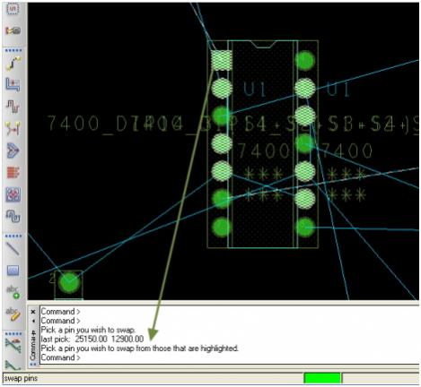
10. Customer Support Recommended—Pin Swapping in Allegro Design Entry CIS and PCB Editor
Naveen Konchada writes for PCB designers and how to automate the tedious task of pin swapping.
Further Reading
In September I listed all of the categories being used by the 68 bloggers at Cadence. If you use any of the Cadence tools or just want to keep updated on the EDA and IP industries, then find and follow your favorite bloggers.
lang: en_US
Share this post via:


Comments
There are no comments yet.
You must register or log in to view/post comments.