

I attended the 3D packaging conference in Burlingame this week. The most interesting presentation to me was by Bryan Black of AMD. He argued very convincingly that Moore’s Law is basically over for the PC microprocessor business and the way forward is going to be 3D. AMD are clearly working on all this.
Increased density and performance/power at each node is great, but in the end it is lower cost transistors that drives the transition for all except the leading edge.
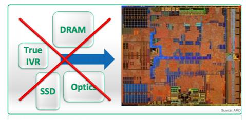
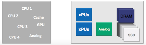
Problem #1: for PCs, everything that can be integrated in the same process has already been integrated. Cache, FPU, multimedia, GPU etc. All that is left is in different process: DRAM, MEMS, storage, optics etc which can’t be integrated onto a mainline digital process.
Problem #2: we are going to go backwards. Next generation processes will no longer support mixed functionality such as analog, cache, high performance, low power.
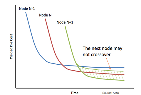
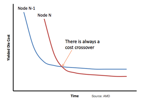
Problem #3: the cost of next generation process may never cross over against current processes so the economic rationale for moving process will stall.
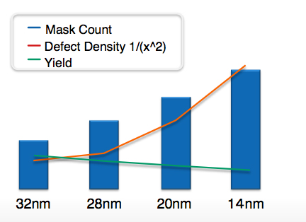
Problem #4: yield is dropping as mask count increases. sweet spot die size is dropping dramatically further lowering yields since microprocessors are large challenging die

Problem #5: more and more of the power budget is going for memory access, leaving less to do actual computation
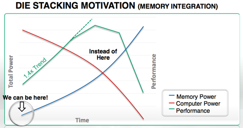
Solution: High-bandwidth memory (HBM) is the first step to getting this under control. Lowers the power needed for memory, freeing up more power for performance. Can continue to scale for years. Can also move analog off and save a dozen mask steps. Can reduce die size to hit reduced sweet spot.
What happens next? Designs are currently running at 100K or so per year using TSV and stacked die and interposers. Next year it will be a million or two. Once the numbers are in the millions, costs will reduce dramatically and a lot of integration will make more sense to do at the packaging level rather than on big SoC like we have been doing. 2014/15 is when 3D ICs become real and start to ship in high volume.
More articles by Paul McLellan…


Real men have fabs!