

The first time that I saw a DRAM in a ceramic package running on a tester I made the mistake of touching my finger to the metal lid, scorching my finger and teaching me a lesson that ICs can run extremely hot. I’ve read a lot the past few years about 3D IC design, and immediately my mind becomes curious about how an engineer would go about simulating or estimating the thermal performance before building a prototype. Last month the Global Semiconductor Association (GSA) invited Gene Matter from Docea Power to talk about:
- How to model a 3D IC for dynamic power and thermal analysis
- Creating compact thermal models for fast simulation and acceptable accuracy
- Performing “what-if” analysis on the floor plan while running real software loads

Gene Matter, Docea Power
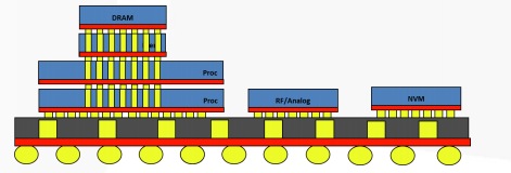
The cross-section of a typical 3D IC may contain a substrate that stacks multiple ICs, like: Processor, DRAM, RF and Non-volatile memory.
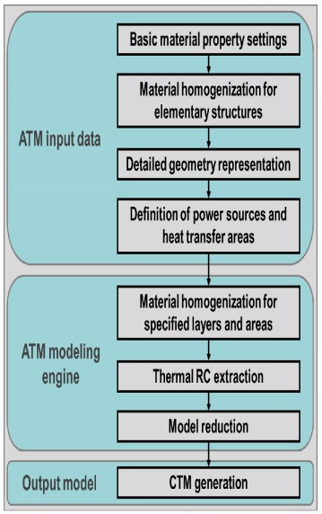
During the design process you want to know how temperature in such a 3D system impacts: power, peak performance, aging, and package costs. Here’s a thermal modeling flow used by Docea Power that creates a Compact Thermal Model (CTM):
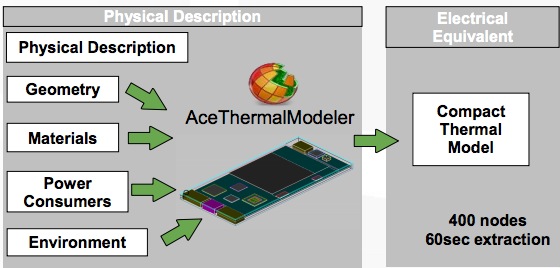
The EDA tool from Docea is called Ace Thermal Modeler (ATM):
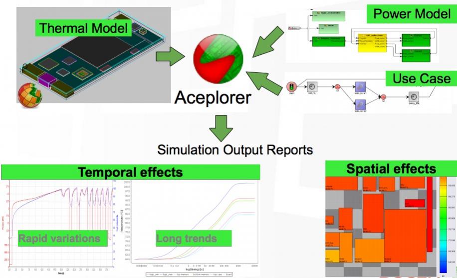
Once you’ve created a thermal model, the next step is to define your power model and use case, then run simulation with Aceplorer to understand the temporal and spatial effects:
By modeling thermal effects at the system level an engineer can now:
- Analyze how IP leakage is temperature-dependent
- Explore multiple power and thermal management strategies
- Qualify the environment capacitive effect
- Qualify the design of minimum cooling properties
- Trade off and explore various floor plan and proximity dependencies
- Find and fix spatial or temporal hot spots and gradients
- Choose an optimal thermal sensor location
- Manage costs across: Die, package, PCB, chassis, the complete system
3D IC Example – WIOMING
Here’s a Memory-on-Logic 3D stack example:
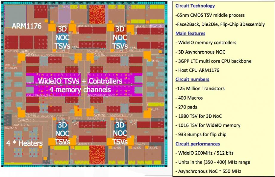
Source:CEA LETI, Pascal Vivet
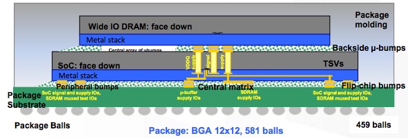
A cross-section view shows how the SoC is connected to the DRAM memory:
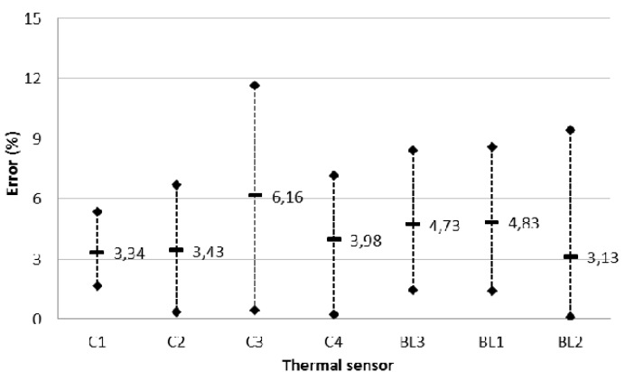
Eight heaters and several thermal sensors were placed around the SoC in order to accurately characterize within about 1 degree Celsius. A compact thermal model was created and static simulation results were generated in milli-seconds, while a dynamic simulation only took seconds to complete. The difference between simulated and measured results across all scenarios showed and average error of just 4.22%:
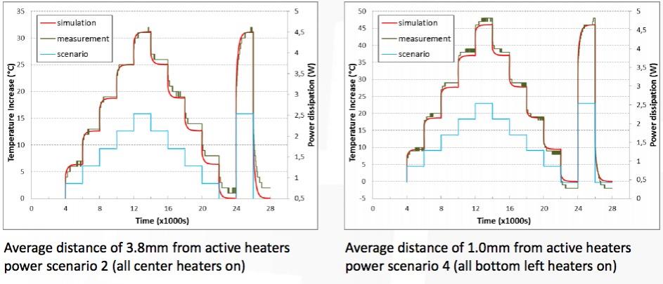
Transient simulation results also showed acceptable correlation between simulated and measured:
Summary
It’s possible to use thermal modeling at the system level with Ace Thermal Modeler to explore and measure a 3D stack with TSVs. Compact thermal models allow for quick run times and decent accuracy. The simulated results correlate well with measured silicon values as seen with the WIOMNG example where a WideIO DRAM was added on top of an SoC.
You may read the complete presentation on the GSA web site.
More Articles by Daniel Payne …..
lang: en_US


The Data Crisis is Unfolding – Are We Ready?