

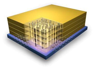
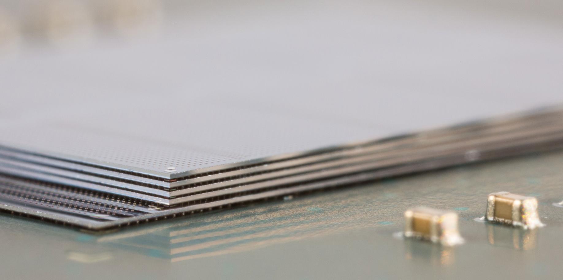
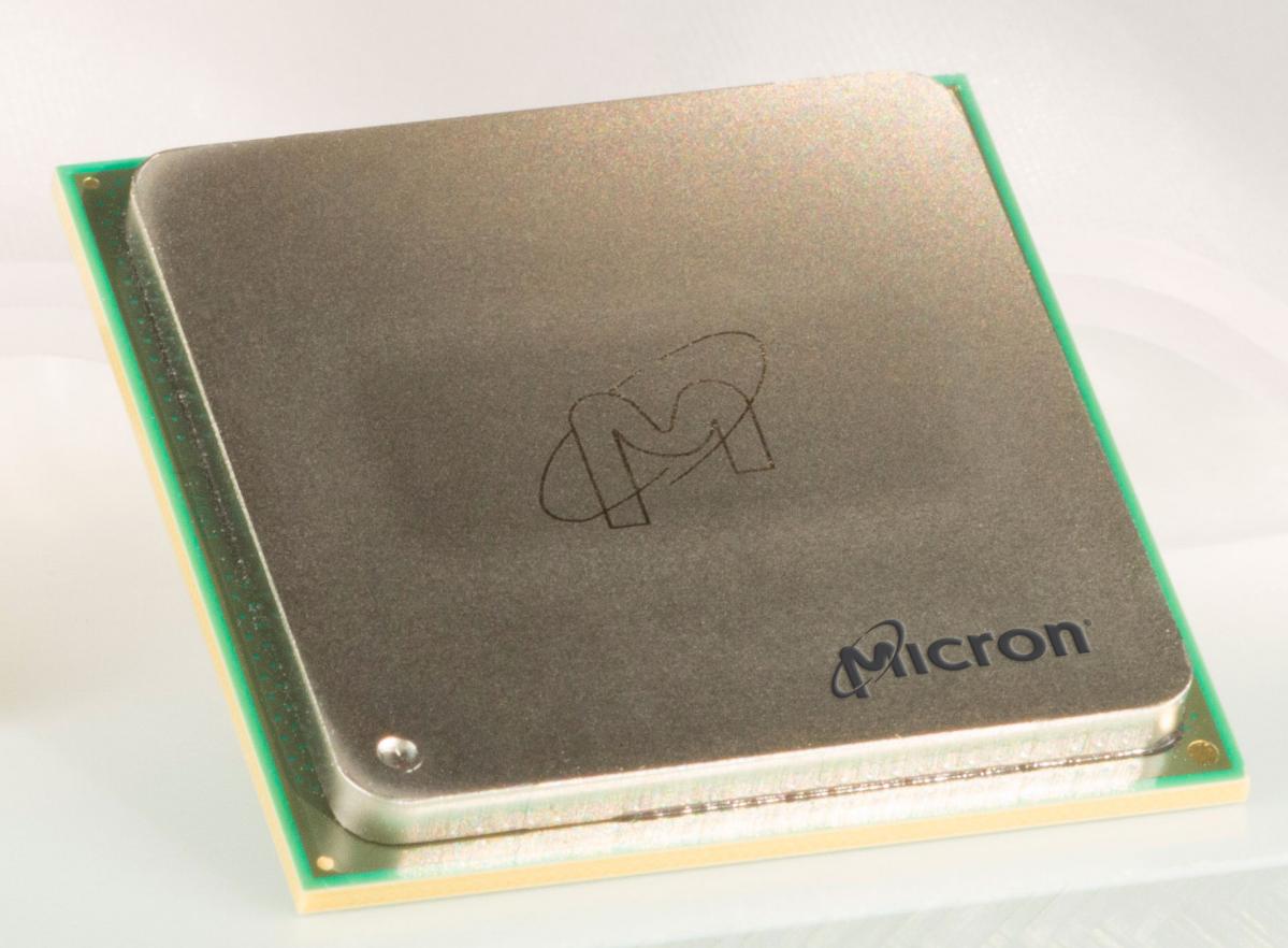
 Today Micron announced that it is shipping 2GB Hybrid Memory Cube (HMC) samples. The HMC is actually 5 stacked die connected with through-silicon-vias (TSVs). The bottom die is a logic chip and is actually manufactured for Micron in an IBM 32nm process (and doesn’t have any TSVs). The other 4 die are 4Gb DRAM die manufactured by Micron themselves with TSVs to for vertical communication. The target market is next generation routers and high performance servers which need memory with very high bandwidth and low power. The HMC can deliver 160GB/s of bandwidth at a power saving compared to normal DRAM of up to 70%.
I talked to Mike Black who is technology strategist for Micron. He said that the work started about 6 years ago when they decided to look at advances in technology since they knew they would want to stack die but to do so required mastering not just making TSVs but creating a whole manufacturing chain for thinning the wafers (without breaking them), bonding everything. Plus the decision to do a system architecture with a powerful logic chip, much more powerful than the type of logic that can be built on a DRAM wafer line.
I think that the announcement today is probably somewhat arbitrary since Micron have been shipping HSC to some partners already. Full production is the second half of 2014.
I think the announcement is interesting for two reasons. One is that the HMC is an interesting device in and of itself. The basic interface is not proprietary to Micron and is defined by the HMC Consortium. Besides Micron, Samsung and SK Hynix are contributors (which covers pretty much the whole DRAM market these days) as are Altera, Xilinx and ARM.
But perhaps even more important for those of us that follow the semiconductor industry in general is that this is a comparatively high volume part using TSVs, so one of the first 3D chips. Of course many people know that Xilinx has been shipping very high end FPGAs using a 2.5D approach on a silicon interposer. But this is not a high volume device and has a price point in the tens of thousands of dollars apparently. Micron are not saying what the price point of the HMC is, but it is clearly a performance, power, cost-of-ownership type of sale meaning that it will cost a lot more than just buying the same amount of DRAM in conventional form.
 Analysts that follow the 3D chip numbers seem to think that use of TSV is going to grow from 1% to 10% by 2017. Since the semiconductor market is roughly $400B that is $40B in 3D chips. Micron reckon their internal numbers are in line with that, at least for the memory markets where they are involved.
Memory turns out to be an ideal pipe-cleaner for 3D since it has redundancy, error correcting codes (ECC), and in this incarnation has a powerful logic chip that can, for example, reconfigure the memory to cope with an open TSV. Also, DRAM doesn’t have the acute power and thermal issues of, say, microprocessors so an HMC is more tolerant of problems and doesn’t stress every aspect of the technology simultaneously.


Huawei’s and SMIC’s Requirement for 5nm Production: Improving Multipatterning Productivity