
One challenge in building a modern SoC is that you want to minimize power, performance and area (PPA) while still getting your chip to market on schedule. Realistically, you can’t actually minimize all of these at once since they are tradeoffs: speeding up a critical path often involves upsizing drivers to larger cells which obviously has a negative effect on area and probably on power too. Sometimes you can get into a virtuous cycle where a block gets smaller, and faster and lower power all at once but that is unusual. Some things, like the floorplan, can have a huge impact on the design but precisely what is not really possible to determine without trying it.
In a modern design, especially early on when there is a lot of flexibility in what can be tried, there can be a huge number of possible changes to consider:
- timing constraints
- target libraries
- floorplan, block aspect ratios
- die size, pin placement, layer assignment
- voltage reduction
- power and clock gating modes
- different RTL coding
- switch soft IP for hard IP
Oasys’ Parallel Implementation Exploration (PIE) allows designers and architects to perform quick “what if” implementation analysis with minimal effort by varying whichever parameters seem most attractive and automatically run all possible combinations of defined input such as clock frequency, voltage, library or aspect ratio. By lowering the cost of evaluating design options and performing them in parallel allows exploration of a much richer space and so homes in on the best option.
PIE works on existing scripts and is very easy to set up. It runs distributed across multiple CPUs with monitoring capabilities to make it easy to track progress. Reports can be generated in Microsoft Excel for comprehensive analysis of the tradeoffs between the various metrics.

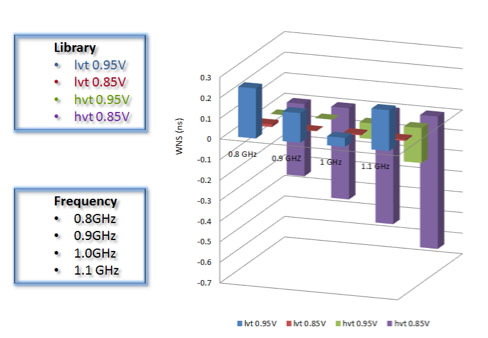
For example, the above graph shows an exploration of a design using 4 different voltages and 4 different frequencies and shows the worst negative slack (WNS) in each case. It is clear that at 1GHz the HVT cells break down and timing is nowhere close to being met.
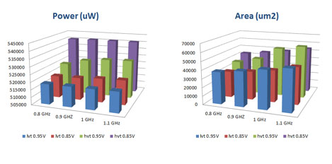
We can also look at the other two components of PPA, the power and area. We can see that the HVT 0.9V library consumes more power and area than the LVT 0.85V library, because the slower cells require more optimization (higher drive etc) to meet timing and so power and area suffer.
The basic technology of Oasys RealTime Designer optimizes at the RTL level resulting in up to 10X faster turnaround times than traditional synthesis tools. Now, with PIE, design teams can leverage server farms to investigate as many implementations as they want and in just a couple of hours home in on the best implementation.


The Data Crisis is Unfolding – Are We Ready?