

 Thermal analysis has traditionally been given short shrift when compared to other more prominent issues facing chip designers. Invarian, to my eye at least, feels that the winds of change are in the air. Not that power or EM/IR issues will fade, that indeed is not the case and in fact quite the contrary, they are contributors to the changing dynamics.
I sat down with Invarian and discussed two test cases, the high and low, so to speak. The first case took us deep inside the bowels of a very large and complex IC. The second case involved the workings at the macro level in dealing with stacked-die configurations. These two cases were chosen by Invarian to demonstrate that thermal analysis is slightly off-center (not unlike our home planet) when compared to the usual suspects in physical verification.
Invarian’s philosophy seems to be that an integrated thermal tool must work from soup to nuts (or the egg to the apples, as the Romans used to say). In other words, to span from the chip world to stacked-die and complex package configurations, all within a single framework. That is Invarian’s value proposition. It’s an interesting approach and certainly a different path than a traditional path for thermal analysis. As for being better, I’ll let the electrons do the thinking for me!
Case A) Thermal Transient Headaches for Network Processor Designs
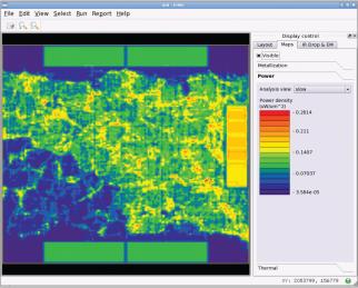
Invarian’s physical analysis tools live at the tail-end of design simulation. They must bridge the gap between generic corner-based electrical simulation and physical reality. Network processors also live at the edge. They are very large high-performance devices designed at leading-edge processes. There is a general consensus that thermal and transient issues will play a larger role as process technology scales downward. What surprised me, not to mention the designers, was that catastrophic thermal transient effects were discovered at the 28nm node. The question is, was this a fluke or a harbinger on things to come?
Working side-by-side with the physical verification team, Invarian was able to demonstrate that issues of this sort get worse. Their AEs have done extensive analysis at 28nm, and have begun 20nm, to specifically analyze the thermal component and it’s effects. The conclusion was that only by taking a holistic approach where thermal analysis was part of an overall plan were errors caught and corrected. Invarian tools provided a framework for concurrent analysis, taking all the effects of power, timing, EM/IR and thermal, which they felt was necessary to get a handle on what they believe will become a major factor for many designs of the future.
Case B) True 3-D Efficient Thermal Simulation for the Micro and the Macro World
Invarian claims that their 3D thermal tool scales from sub-transistor levels to complex stacked-die configurations. Working with CAD engineering and packaging groups to solve 3D electro-thermal and mechanical stress challenges, they believe, requires an ability to scale up for gathering data, scale down for pinpoint analysis, an ability to generate ‘real-world’ activity, and to do all this quickly and efficiently. It certainly is a big challenge.
Modeling the total environment is a necessary condition, according to Invarian, for capturing enough data for accurate analysis of electro-thermal transients. And there are no thermal tools, at least that I know of, available on the market that scale from the packaging world down to the TCAD level. An important feature of this tool, in my opinion, is its ability to build an optimal thermal grid for the solver.
A natural progression to 3D transistors, low-k dielectric materials and stacked-die configurations is pushing the market for better 3D thermal analysis tools. What began, as an R&D effort with Invarian’s high-performance and mobile customers, seems to be steadily moving toward design engineering. At its heart, Invarian makes a basic assumption, and that is that physically correct models are necessary to get accurate temperature results. In addition, they believe that the tool must easily transverse between the macro world and the micro world. Activity data can also play a critical role in ‘hot spot’ thermal management. What I have learned is that efficient 3D thermal tools must not only generate accurate results in a timely manner, they must also navigate between the various design and research centers within an organization.
InVar Pioneer Thermal™provides the industry’s largest capacity and most accurate thermal sign-off analysis available today. Invarian solves the problem of miscorrelation with a unique approach to thermal analysis. Different analysis engines work in concert and take into account the interdependence of power, timing, voltage, and temperature into account. Contrary to other tools, all types of analysis are performed in a continuous temperature/voltage space across the chip. InVar does not use predefined corners for analysis.
Invarian is an Exhibitor at DAC, June 2-6, 2013 – Austin, TX – Booth # 1332. On hand will be experts to discuss all the various aspects of physical verification and give a sneak-preview of upcoming products in the areas of ESD and In-rush.
lang: en_US


The Data Crisis is Unfolding – Are We Ready?