

My IC design career started at Intel with DRAM chips, so I’m very familiar with clockless design because we used self-timed techniques to get maximum performance. I remember blogging about an asynchronous design company called Tiempo back in 2010, while blogging at Chip Design Magazine. A few weeks ago there was a press release that caught me eye: French Consortium Announces Development of a Clockless SMARTcard chip. Steve Svoboda is my contact at Tiempo and he sent me an email, which turned into a blog interview to satisfy my curiosity.


Steve Svoboda, Tiempo
Interview
Q: Why did the partners choose a clockless design approach?
The partners (Tiempo, Gemalto, CEA-Leti, Invia, Presto Engineering, and L Foundry) wanted to explore ways to generate the next level “breakthrough” in performance for contactless smartcards, while achieving equivalent or higher security. Tiempo proposed that using their technology to develop a clockless smartcard chip, the partners could realize a chip with substantially higher performance than other chips currently on the market, along with greater security and resistance to hacking, and monitoring attacks.
Q: What benefits did clockless provide that the previous chip approach did not?
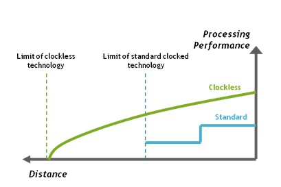
In contactless smartcards, the chip is powered by the magnetic field strength received from the reader. This field strength varies with the cube of the reader-distance (making it extremely sensitive to the distance from the reader), as well as the orientation of the card relative to the reader (the card must be parallel to the reader for maximum field strength.)
The clockless chip Tiempo developed for the ASMART project should run at substantially higher speeds than conventional chips on the market today, with equal or lower magnetic field strength from the reader. In addition, the speed of the clockless chip is able to vary dynamically and continuously as the magnetic field strength would vary.
These technical advantages would enable OEMs using the chip to deliver contactless smartcards that process transactions faster, and more reliably (i.e. not requiring “reswipes” as often) than contactless smartcards currently on the market, without making any compromises on the security of executed transactions.
Q: How long was this design project from concept to tape-out?
ASMART is an ongoing multi-phase project, with delivery of progressively more advanced prototypes scheduled at the end of each phase. For security reasons, the effort/scope of the different phases in the project remains confidential. However the partners can say the design effort so far has never exceeded that for a conventional synchronous design (i.e., using a clockless approach has not added to the cost, labor effort, or schedule of the project.)
Q: What were the design challenges, and how was each challenge met?
The main design challenges were related to the “front-end”, i.e. modeling/synthesis, functional verification, and test.
The Tiempo team modeled the entire digital portion of the chip in System Verilog, and then used Tiempo’s Asynchronous Circuit Compiler (“ACC”) synthesis tool to generate gates.
Functional verification was performed with the SystemVerilog and gate-level models, using Synopsys VCS.
Test was also challenging, as the design was entirely clockless. Tools for automatically inserting DFT for clockless designs don’t yet exist today, so Tiempo engineers had to rely on a handcrafted approach, heavily based on functional-test: in this circuit, test was almost entirely based on BIST.
Notably, the clockless, delay-insensitive nature of the logic proved a big advantage during the backend stage, as timing-closure became much more simple/straightforward than would have been the case with a conventional-logic clocked design. Integration of the Digital with the Analog/RF portions is substantially easier due to the clockless nature of the digital logic (much reduced interference, and much smoother/more uniform power consumption.)
Q: Which specific tools were used?
Modeling – SystemVerilog
Synthesis – Asynchronous Circuit Compiler (Tiempo)
Verification – VCS (Synopsys)
Place & Route – IC Compiler (Synopsys)
Q: What did the design team learn along the way?
The team learned:
– how to apply a delay-insensitive, clockless design flow in the context of developing an entire SoC.
– how clockless design makes backend timing-closure much easier than with equivalent synchronous logic.
Summary
It looks like Tiempo is finding it’s way in the world by becoming more of an IP company than an EDA company. They were able to create an EDA tool flow from tools that expected a clocked methodology, plus added their own for logic synthesis.
lang: en_US


The Data Crisis is Unfolding – Are We Ready?