

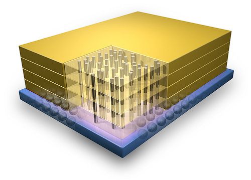
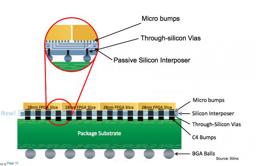
 For the last few years, thru silicon via (TSV) based ICs have been looming in the mist of the future. Just how far ahead are they? Xiliinx famously has a high-end gate-array in production on a 2.5D interposer, Micron has a memory cube, TSMC has done various things in 3D that it calls CoWoS (chip on wafer on substrate), Qualcomm have been working in the area for years, Cadence has talked about several tapeouts. Is it finally going to be real? More than Moore, which used to apply to these types of technologies, going vertical seems to have been somewhat hijacked already to apply to almost anything.
One school of thought is that if you can go the Moore route, going to 20nm or 14nm, then that is the way to go. I’m not even sure about that. At one 3D working group I attended, a guy from eSilicon used their cost model to estimate that Xilinx were saving 80% of the cost by using a 2.5D interposer based approach versus trying to yield such a big die (probably the maximum reticle size) in an immature process.
 But once you start to want to mix technologies such as RF and analog, it is difficult to put them on the same wafer and the More route starts to have its attractions. I’ve talked to a few people about analog in the FinFET era and the received wisdom is that you can do some stuff but it is really hard. You have quantized transistor sizes so you can’t always get the ratio you want. But for sure you can put an analog die on an interposer with a FinFET. And you can put DRAM on logic, even lots of DRAM maybe.
There have been some technical issues but the main issue now is whether it is cost-effective compared to other forms of integration.
At EDPS on Thursday Herb Reiter will moderate a session on 3D IC design. The other presenters are:
- Dusan Petranovic of Mentor, looking at verification
- Brandon Wang of Cadence, focused on implementation
- Mike Black from Micron, the strategist behind their memory cube
- Gene Jacubowski of E-system Design, signal and power simulation
EDPS is in Monterey next Thursday and Friday, April 18th and 19th. The full program is here. Registration is hereand use the promo code SemiWiki-EDPS-JFR to save $50.. Call the hotel directly for room reservations.


The Data Crisis is Unfolding – Are We Ready?