
I read two blogs this week that got me to thinking about contingencies in SoC implementation. By contingency I mean using an EDA tool flow from the leading vendor for logic synthesis and then discovering that you cannot route the design without expanding the die size after a few weeks of concerted effort, then having to come up with a Plan B. The blogs were from two people at Oasys Design Systems:

This AE named Ganesh Venkataramani talks about visiting a semi company in the mobile market that had a chip in tape-out that was growing too large because of congestion. They couldn’t even fit the whole chip into their logic synthesis tool at one time, so that made it tough to figure out if there were any top-level timing issues.

Large SoC design teams have separate front-end and back-end engineers that perform very different tasks with different logical and physical IC design tools. This particular design team decided to give Oasys tools a shot on resolving their routing congestion dilema, I mean what did they have to lose?
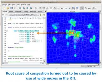
With the help of the AE they were able to get their design loaded into Oasys tools in a day. The physical synthesis tool is called RealTime Explorer, and it could synthesize the entire SoC in a couple of hours. Next, they visualized the results by cross-probing between the routed IC layout and RTL source code to identify the source of congestion. Plan B worked out quite well for this design team because now they had pin-pointed their routing congestion back to the RTL where wide muxes had been used. Pretty impressive for just one day’s work compared to previous efforts that fell short after weeks with multiple engineers.
The second blog was written by Dan Ganousis, an EDA veteran who started out as a design engineer just one year prior to me back in the 1970’s. His blog also focuses on the implementation issue of routing congestion.

So what happens when the front-end RTL team assembles all their IP, writes new code, verifies the logic, does some logic synthesis, then throws the design over the wall to the back-end IC implementation team? Often the result is an IC design deemed “Unroutable”. The good news is that using an EDA tool like RealTime Explorer can let you cross-probe between the physical and logical worlds:
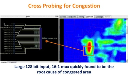
The screenshot above shows the physical routing congestion on the right, where Red is the area of highest routing congestion. The cross-probing lets you quickly identify the RTL source code responsible for causing this congestion, so now you know what to modify in RTL to improve your physical layout.
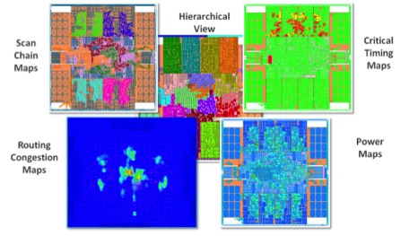
Here’s the big picture view of analysis features that you’ll find in RealTime Explorer:
Summary
If your present EDA tool flow isn’t creating the chip size that you want, or getting out of tape-out quickly enough, then consider calling Ganesh as your Plan B.


The Data Crisis is Unfolding – Are We Ready?