

TSMC and Synopsys hosted a webinar in December on this topic of double patterning and how it impacts the IC extraction flow. The 20nm process node has IC layout geometries so closely spaced that the traditional optical-based lithography cannot be used, instead lower layers like Poly and Metal 1 require a new approach of using two masks per layer. Using Extreme UltraViolet (EUV) with it’s shorter wavelength could get us back to 1 mask per layout layer, however EUV is not ready for production use quite yet.
 Anderson Chiu presented from TSMC, and he is a technical manager of Design Infrastructure Marketing Division of Design and Technology Platform/R&D, responsible for EDA marketing. He is the program owner of TSMC 20nm Reference Flow, CoWoS Reference Flow, EDA tool certification program and Integrated Sign-Off Flow program. He has 10 years experience in chip design & flow methodology. Anderson received his MS and BS in Computer Science and Engineering from Chung-Yuan Christian University in Taiwan.
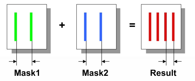
When using two masks per layer (Double Patterning Technology, DPT) there is an issue of mask alignment where any mis-alignment will cause layer spacing values to change, therefore changing the parasitic coupling capacitance values.
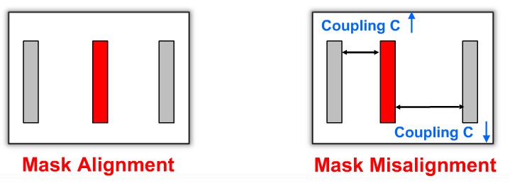
Shown above on the left is perfect mask alignment and the center conductor (Red) has an equal spacing to the conductor on the left and ride sides. However on the right is shown what happens if there is a mis-alignment of one mask which shifts the center conductor (Red) closer to the left conductor thus increasing that parasitic capacitance value. Likewise, the capacitance from center to right conductor would decrease with this mis-alignment. So at 20nm we are adding more variation corners caused by DPT effects.
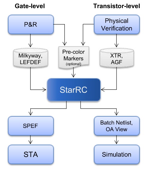
The EDA design flow needs to be updated to support DPT as shown below:
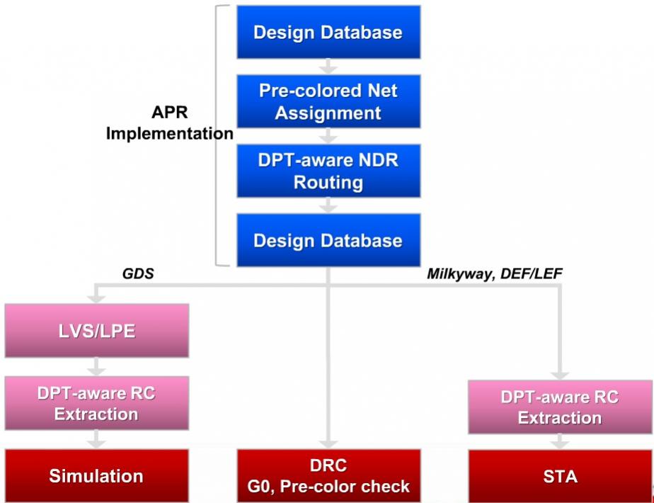
APR is the Automatic Place and Route tools. LVS/LPE is Layout Versus Schematic checking, and LPE is Layout Parasitic Extraction. DRC is Design Rule Checking. STA is Static Timing Analysis.
TSMC has worked closely with Synopsys to ensure that at 20nm the new DPT requirements have been added to each EDA tool:
- Place and Route (IC Compiler)
- Parasitic extraction of R and C values (Star RC)
- Design Rule Checking (IC Validator)
- Static Timing Analysis (PrimeTime)
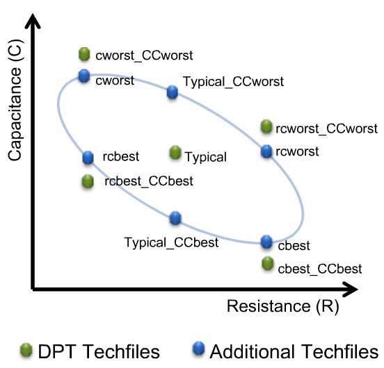
Five new corners are added in a DPT flow to account for RC variations:
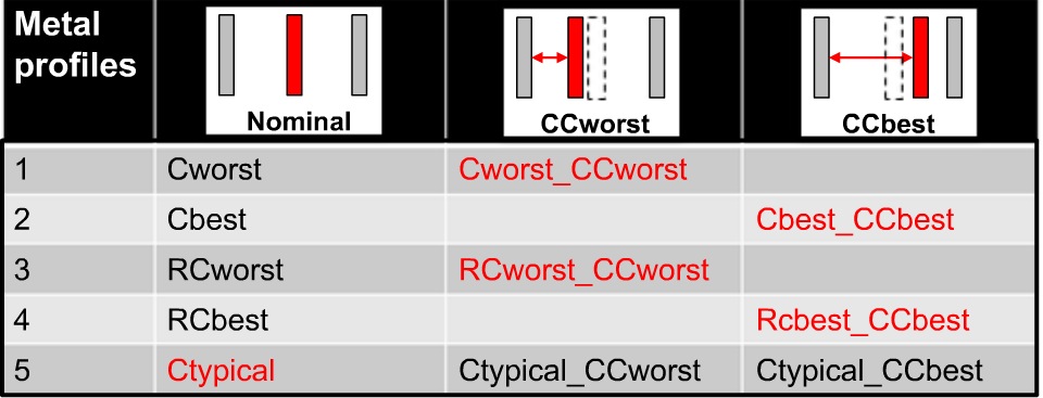
Setup time sign-off would use: Cworst_CCworst / RCworst_CCworst
Hold time sign-off would use: Cbest_CCbest / RCbest_CCbest / Cworst_CCworst / RCworst_CCworst
 Beifan Qiu from Synopsys is a senior R&D manager for the StarRC extraction tool. She has worked in parasitic extraction, physical verification and DFM areas for more than fifteen years. Beifang received her MS in Electrical Engineering from Vanderbilt University and BS in Electrical Engineering from Shanghai Jiao Tong University in China.
Beifan started out with the main equation used in lithography as it applies to critical dimensions, or the narrowest line that you can manufacture:
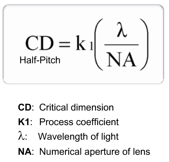
The fab equipment is using 193nm (Lambda) light sources, max NA is 1.35, and the smallest K1 value is 0.25, so the limit of single patterning is about 72nm. The smallest half pitches are :
- 40nm (at 22nm)
- 32nm (at 20m)
Using DPT at 20nm is more expensive than previous nodes because more mask layers and steps are required.
The variation effects of DPT mask mis-alignment is automatically taken into account by adding new corners for evaluation. The largest variation in capacitance values happens at minimum spacing of interconnect. At 20nm the average impact on coupling capacitance across all nest is about 2-3% compared to nominal capacitance.
If you have critical nets you may choose to pre-color your interconnect, therefore forcing that interconnect onto the same layer and avoiding the DPT variation issues:
You can use the five basic corners to model the DPT effects, or add up to six more corners for advanced analysis:
StarRC does support multi-corner extraction that can create multi-valued SPEF files for use in the Static Timing Analysis tool, PrimeTime. Running StarRC with multi-corner can speed up results by 3X by evaluating all corners simultaneously.
Q&A
Q: How many corners are really needed to model DPT effects?
A: Five corners are added to model DPT accurately.
Q: Are there any run-time impacts or memory penalties during extraction?
A: No run-time slow downs for DPT. Reading the IC layout can slow down with markers being added.
Q: Which tech files do I import?
A: You can import the new DPT tech files for greatest accuracy.
Q: How do I define additional design margin?
A: Using StarRC full color with all combinations. Ask TSMC field support for more details.
Q: Which version of ICC should I use for the DPT flow?
A: Version 12.12 has direct read for the DPT flow.
Summary
It takes tight collaboration between foundry and EDA vendors to implement DPT in a 20nm IC design flow. Most of the effects of DPT have been automated inside of each EDA tool, so the IC designer can come up to speed quickly.


Comments
0 Replies to “Double Patterning for IC Design, Extraction and Signoff”
You must register or log in to view/post comments.