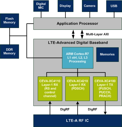

ARM and CEVA have launched a white paper, addressing one of the hottest topics of the day: LTE-Advanced modem architecture. This very exhaustive paper, written by David Maidment (Mobile Segment Manager, ARM), Chris Turner (Senior Product Manager, ARM) and Eyal Bergman (VP Product Marketing, Baseband & Connectivity, CEVA Inc.) explains how Designing an efficient LTE-Advanced modem architecture with ARM[SUP]®[/SUP] Cortex™-R7 MPCore™ and CEVA XC4000 processors. The title is self-explaining, but having a look at the high level architecture allow to identify which core does what task. The Cortex-R7 does L1 control and L2, L3 processing, when no less than three CEVA-XC4000 DSP cores are in charge of the Layer-1 RX (XC4110 and XC4210) and TX (XC4100 on the right).

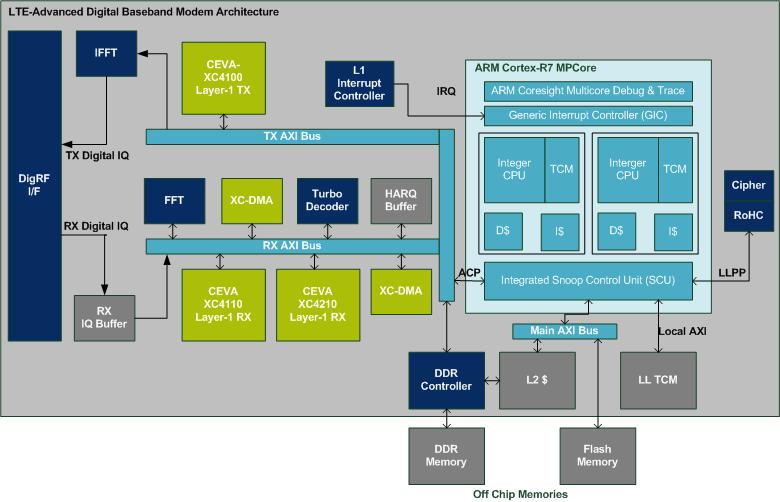
This LTE-Advanced Digital Modem Architecture is precisely described in this very comprehensive white paper, as we can see with this more detailed description, showing the AMBA AXI busses, the hardened FFT, Turbo Decoded, XC-DMA, Cipher RoHC, L1 Interrupt Controller, IFFT and DDR Controller functions.
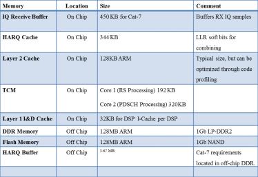
In such a complex, multi-core design, the memory utilization and assignment is a key architecture decision. The table below summarizes both the size and the location (on chip or off chip) of the various memory blocks.
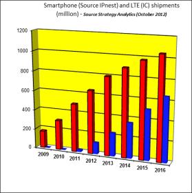
Let’s take a minute to have a look at the LTE penetration forecast for the next 5 years (in red) to be compared with the smartphone shipments (in blue). LTE adoption growth rate is impressive, and the “feeling” can be confirmed by facts (extracted from the white paper):
“The LTE (Long-Term Evolution) standard was first ratified by 3GPP in Release-8 at December 2008 and was conceived to provide wireless broadband access using an entirely packet based protocol and was the basis for the first wave of LTE equipment. LTE has now been adopted by over 347 carriers in 104 countries (Ref GSA) including such territories as USA, Japan, Korea and China to name but a few, making it the fastest adopted wireless technology in history”
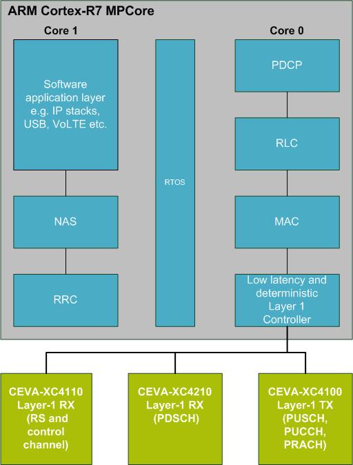
And, because the SW development can not be separated anymore from the HW development, the SW mapping is completely described in the article, as we can see per the picture below:
You will find a lot more information by reading the complete white paper, you will find it here.
Eric Esteve from IPNEST
Share this post via:


Comments
0 Replies to “When ARM and CEVA team-up for “Designing a Multi-core LTE-A Modem””
You must register or log in to view/post comments.