
Last month at DAC I learned how IBM, Cadence, ARM, GLOBALFOUNDRIES and Samsung approach the challenges of SoC design, EDA design and fabrication at the 20nm node. Today I followed up by reading a white paper on 20nm IC design challenges authored by Cadence, a welcome relief to the previous marketing mantra of EDA 360.
Here’s a quick overview of the challenges, approaches to overcome the challenges and then the impact.
[TABLE] style=”width: 650px”
|-
| Challenges
| Approach
| Impact
|-
| Lithography
| Double Patterning Technology (DPT)
| More masks, mask costs of $5M to $8M, new DPT-aware EDA tools, new DPT-aware cells and IP,
|-
| Variability
| Early analysis of Layout Dependent Effects (LDE)
| New EDA tool flows, new design rules
|-
| Design Complexity
| Re-use IP, more verification, mixed-signal design, 3D, TSV
| Longer schedules, AMS tools required, SoC design costs $120M – $500M
|-
Benefits of 20nm
With these challenges at 20nm versus 28nm the goal is to exploit the technology with products that have:
- 30-50% performance improvement
- 30% dynamic power savings
- 50% area reduction
- Up to 12 billion transistors
Lithography
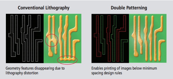
A picture is worth 1,000 words so here’s the story of why we need to use two masks for a single layer in order to resolve the patterns in silicon:

On the left is what happens when using a single mask and trying to produce small patterns at 20nm dimensions, while on the right is the much improved manufacturing result when using two masks for the same layer. With DPT each complex layout pattern is separated with enough spacing to allow the 192nm lithography equipment to adequately resolve without interference from neighboring patterns. Only the lowest mask layers in 20nm require this special treatment, but it will cost you more in mask expenses.
All of the EDA tools that create IC layout must be updated to take into account how to create DPT patterns. Once you’ve made something like a standard cell, then you need to ensure that when that cell is placed, flipped or mirrored, that it still is DPT compliant:
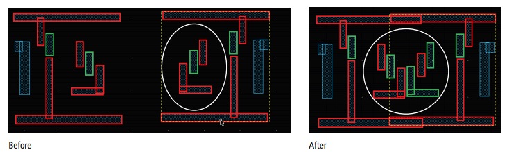
In the above layout the layer has been colorized into red and green, denoting the two different masks required for DPT. With new automation the IC designer doesn’t have to think about how to make their IC layout DPT compliant, because a manual coloring would be too tedious and error prone.
Connecting the standard cells together is done by a Place and Route tool, so it needs to be updated to become DPT aware as well.
Extraction tools read these layouts to create a netlist for either circuit simulation or static timing analysis, and with DPT awareness it will take into account mask offsets that change the parasitic R, C and L values.
The DRC tools likewise have to take into account the hundreds of new rules at 20nm
Variability
The foundries want high yield and to ensure that yield they characterize the silicon and produce layout rules that need to be followed by layout and circuit designers. At 20nm you can expect about 5,000 design rule checks (DRC). What’s new at 20nm compared to 28nm are about 40 rules for DPT and 400 rules for things like layout directional orientation, transistor proximity and inter-digitation patterns.
Variations in the actual layout across the die need to be taken into account and simulated prior to tapeout, this means more circuit simulation, stating timing analysis, and statistical timing analysis. With 20nm there can be more coupling between nets and that will in turn impact sensitive analog circuits or memory cells.
One Layout Dependent Effect is how the Voltage Threshold (Vt) of an MOS device changes based on the proximity to the well layer:
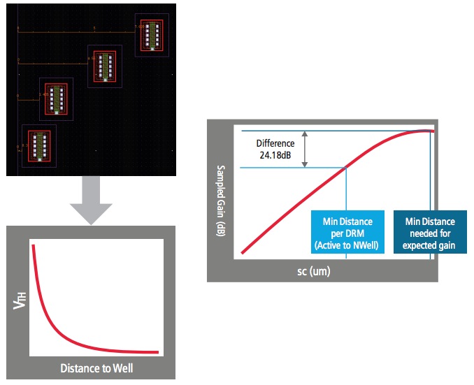
In this diagram the MOS transistor is show at the top, and as the transistor is placed closer to the well the value of Vt goes up. This variation in Vt will impact the gain and speed of the transistor, so on the right is a chart showing the gain of the transistor and the design rule manual (DRM) recommendation for a safe spacing, active to NWell.
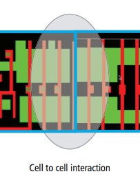
Even the placement of standard cells will trigger layout dependent effects that impact timing:
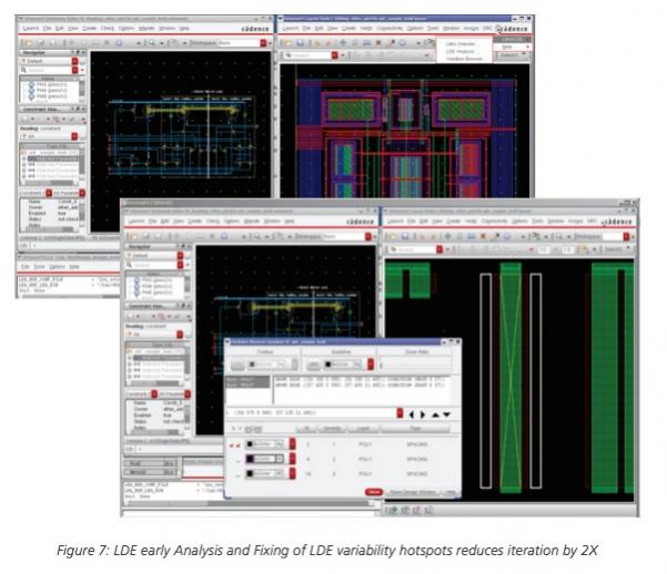
The good news is that all of these effects can be analyzed early in the design process through tools that have been made LDE aware:
Design Complexity
Sequential IC design flows have given way to concurrent design flows where the goal is to Prevent, Analyze and Optimize. Specific examples of this approach include:
- Constraint-driven design
- LDE aware placement
- Color-aware place and route
- In-design verification
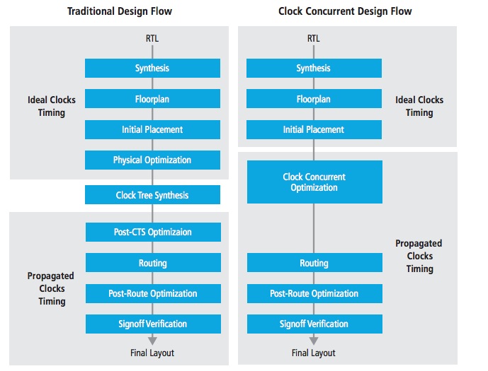
Power, Performance and Area (PPA) goals define each SoC spec, and to meet specs you need to support complex clocking, multiple power domains, and automated low power techniques. One such approach is called clock concurrent design where concurrent optimization is used:
Summary
Cadence has been collaborating with foundries (IBM, GLOBALFOUNDRIES, Samsung, TSMC) at the earliest development stages of 20nm and below nodes to update the IC tool flows to ensure an automated approach to SoC design that follows a methodology of Prevent, Analyze and Optimize.


Comments
0 Replies to “An Approach to 20nm IC Design”
You must register or log in to view/post comments.