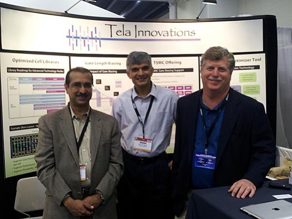

Rajiv Bhateja, Dhrumil Gandhi and Neal Carney met with me at DAC on Wednesday to give an update on what’s new in 2012 for Tela Innovations, a provider of lithography optimized IP and tools. This team has a rich history in EDA and IP from companies like: ARM, Artisan, Mentor Graphics and Silicon Compilers.

Notes
What’s New?
Two businesses – acquired Blaze DFM in 2009, optimized layout for restrictive design with DPT.
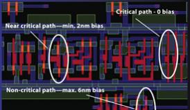
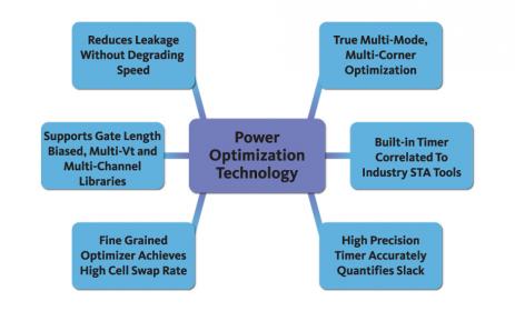
Blaze DFM – technology licensed to TSMC for gate length biasing, being used at 28nm now both positive (less leakage) and negative biasing (faster). Less timing critical paths can use positive bias.
TSMC – promotes channel length modulation. Then IP suppliers like ARM and Synopsys design cells to allow this capability.
Tela can directly work with SOC designers to use their software to swap out cells for lower leakage or faster speeds.
Tela – has done over 100 tapeouts. Mellanox (10G Phy), LSI Logic (media), Samsung (multiple). 25 different customers have used this at TSMC however legally cannot disclose all the names.
Leakage at newer nodes continues to increase in severity. 40nm causes a surge of business for Tela. Customers come back for repeat business.
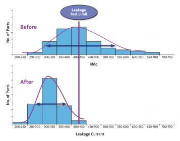
Leakage variability is increased if the gate edges are rougher.
For fastest speeds use the shortest gate lengths, however on paths that are non-critical then back off on channel lengths while maintaining cell footprints.
Success in 12 months – continued adoption of gate biasing at 28nm (about double the designs compared to 40nm).
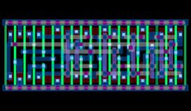
Optimized Cell LIbraries – knowing what the lithography tools can produce with high yield, then optimize the topology to conform to best litho practices. Customers would get a GDS II cell library, then do their own cell characterization. Customers cannot be named, stay tuned. 32nm, 28nm and 20nm layouts.
Over 70 patents issued.
Cell swapping is done best by Tela at a very fine level using their timing analysis.


The Data Crisis is Unfolding – Are We Ready?