

At the GSA 3D IC working group meeting, Cadence presented their perspective on 3D ICs. Their view will turn out to be important since the new chair of the 3D IC working group is going to be Ken Potts of Cadence. Once GSA decided the position could not be funded then an independent consultant like Herb Reiter had to bow out and the position would need to be taken by someone funded by the company they work for. So thanks Cadence. And thanks for the beer and wine after the meeting too.
Ken would have been there but unfortunately he has broken both his elbows (get well soon Ken) and driving over 17 from Santa Cruz is dangerous enough with both arms working. I know Ken from both Compass and my own Cadence days. He also owns a car repair shop in Santa Cruz with his family but somehow the gravitational attraction of EDA pulled him back in.
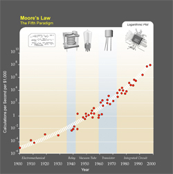 John Murphy presented Cadence’s perspective. First, Murph pointed out that Moore’s law has been going on for a century. I’ve pointed this out before, indeed we both used the same graphic stolen from Ray Kurzweil that covers 5 technologies (mechanical, relay, tube, transistor, IC). From the system performance point of view, if not from the purist view of lithographic advance, this is likely to continue for the forseeable future.
Cadence sees two “killer apps” for 3D-IC in the short term.
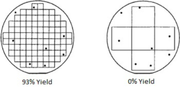
The first is yield enhancement. The same defect density has a huge impact on yield depending on die size, so there are is a lot of upside to building a system out of several smaller die versus one huge one. Indeed, this is the motivation for Xilinx’s excursion into 3D (2.5D on silicon interposer). eSilicon used their own cost models to estimate that Xilinx is getting a huge bump in yield. And as Liam Madden of Xilinx had pointed out earlier in the day, they don’t need to put all the slowest die on one interposer so there is a performance gain too, since all 4 slices are never worst case as might happen with a single large die (processed with slightly too long gate lengths). This shows it graphically (obviously exaggerated, nobody is making 4″ chips, too big for the reticle anyway).
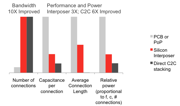
The second killer app is memory subsystem, where by putting memory on logic (or stacks of memory on logic) the power can be significantly reduced while the performance is increased.
Cadence claim that they have 8 test chips and 1 in production (Altera). In fact they said there is a second production design but they cannot say with who. One thing that is clear is that 3D requires a lot of cooperation between a lot of different partners, not just in EDA. In fact, designing a 3D IC is not that different from designing several separate ICs. Yes, some new stuff for TSVs is required, and test is complicated. But it is nothing compared to what the OSATs have to do: putting a 3D chip stack together is nothing like just putting a chip on a BGA with a whole new set of challenges to do with alignment, not breaking the very thin die, bonding and debonding them from something to make the handleable, making all the microball connnections and so on.
Like everyone else, Cadence sees 3D coming as a series of steps. First 2.5D silicon interposer designs, then logic on memory with true 3D some way off.


Comments
There are no comments yet.
You must register or log in to view/post comments.