
Nandu Bhagwan is CEO of GHz Circuits and has been designing PLL circuits used in ICs for the past 12 years. Mr. Bhagwan did a video interview with John Pierce of Cadence to talk about the challenges of PLL design.

Nandu Bahgwan, GHz Circuits
Here’s a block diagram of what goes into most digital PLL designs:
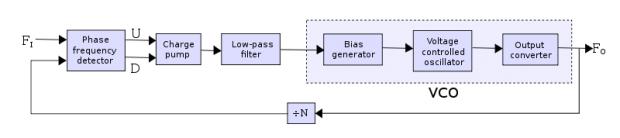
Source: Wikipedia
An input clock is supplied on the left-hand side called F1 and the resulting output clock on the right-hand side called Fo is in-phase with F1 and can be the same frequency or some multiple of it. Applications of PLL include:
- Clock Recovery
- Deskewing
- Clock Generation
- Spread specturm
- Clock Distribution
- Frequency Synthesis
Q: What are your PLL design challenges?
A: Our consulting company does PLL design work. Each new node makes PLL design more challenging. The immense amount of simulation time is an issue for us. A week long transient noise analysis is just too long, so instead we abstract the analysis.
Q: What kind of specs do you have for PLL designs?
A: Random jitter of less than .5 ps is on PLL spec we need to meet, however it will take one week of simulation using an 8 core machine at the SPICE level. We need to use high accuracy tolerances. We build models of each PLL building block using equations in order to abstract PLL behavior, this allows much faster simulation times.
Q: How sophisticate are these PLL models?
A: We model both 2nd order and 3rd order effects in our equations. Now we can iterate quickly instead of waiting a week.
Q: Where can I go to read more about how you model and simulate PLL designs?
A: Our web site has papers on PLL simulation, modeling and technology.
Summary
PLL circuit design does start out with transistor-level schematics, includes SPICE simulation, and finally you can model each block within a PLL with equations for significant speed-ups in analysis run times (4 orders of magnitude).


Comments
There are no comments yet.
You must register or log in to view/post comments.