

3D and 2.5D (silicon interposer) designs create new challenges for EDA. Not all of them are in the most obvious areas. Mentor has an interesting presentation on what is required for verification and testing of these types of designs. Obviously it is somewhat Mentor-centric but in laying out the challenges it is pretty much agnostic.
The four big challenges that are identified are:
- physical verification for multi-chip packages using silicon interposers and (through-silicon-vias) TSVs.
- layout-versus-schematic (LVS) checking of 3D stacks, including inter-die connectivity
- parasitic extraction for silicon interposers and TSVs
- manufacturing test of 3D stack from external pins
The first 3 challenges, updating the physical verification flow to handle 3D, are incremental improvements on existing technology. One complication is that the technologies (and hence the rules) used on each die may be different. But fundamentally, physical verification can be done one die at a time, LVS is comparing networks although bigger and more complex, and parasitic extraction can be done one die at a time although there are also inter-die effects that may need to be modeled. One area that does require a lot more attention is ensuring that the TSVs on one die do indeed match up to appropriate connection points on the die underneath so circuit extraction cannot be done entirely one die at a time.
The entire manufacturing process is obviously impacted by 3D in a major way. But here’s one less obvious area that is impacted: wafer sort. When a wafer comes out of the fab and before it is cut up into individual dice, it is tested to identify which die are good and which are bad. But at some point, enough testing is counterproductive: it is cheaper to waste money packaging up a few bad die and then discarding them at final test, than it is to have a much longer wafer test (perhaps even requiring more testers). When you discard a bad die at final test you are just wasting the cost of the package and the cost of assembly. The die itself was always bad.
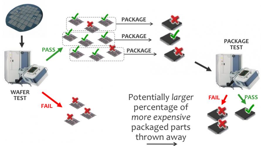 With 3D this tradeoff point moves. If you package up a bad die along with several good die in a stack, then not only are you discarding a bad die, the package and the assembly cost. You are discarding all the other die in the package which are (most likely) good. So it makes sense to put a lot more effort into wafer sort. Plus, to make it worse, this is more likely to happen since, with several die in the package, the chance that all of them are good is lower than the chance that any one die is good.
Once the die are packaged up, then the challenge is to get test vectors to any die that are not directly connected to package pins. A very disciplined approach is required to ensure that vectors can be elevated up from the lowest die (typically connected to the package) and the upper levels.
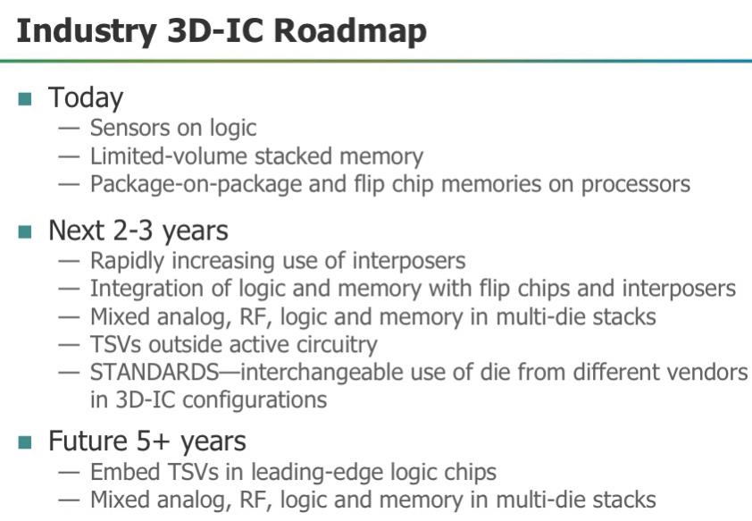
Future challenges that are identified are:
- architectural exploration. 3D offers another degree of freedom and all the usual floorplanning issues have to be extended to cover multiple-floors
- thermal issues and signoff. TSVs and multiple die spread out heat to some extent, but nevertheless all the heat from the middle of the stack needs to get out
- physical stress especially in areas around TSVs (where the manufacturing process can affect transistor threshold voltages)
The Mentor presentation is here.


Comments
0 Replies to “Going up…3D IC design tools”
You must register or log in to view/post comments.