

One of the challenges of designing a modern SoC is that the digital parts of the circuit are really something that in an ideal world you’d keep as far away from the analog as possible. The digital parts of the circuit generate large amounts of noise, especially in the power supply and in the substrate, two areas where it is impossible to completely keep the analog and digital apart. Ideally, from a noise point of view, we’d continue to put the digital and analog on separate chips (so no shared substrate and minimal power supply coupling) but from a cost point of view we have to put them on the same chip and analyze the consequences.
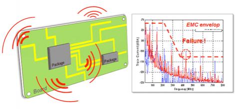 The existing static approaches to this problem, modelling the problem as IR drop in the power supply, have run out of steam for these SoCs with layers of power reduction techniques, and are lacking in both accuracy and capacity for analyzing the effects of transient power supply noise. Trying to do dynamic analysis using SPICE simulators runs into capacity limitations and using a simplified netlist reduces accuracy unacceptably. Substrate noise injection is a chip-wide phenomenon. Getting the analysis wrong can lead to expensive re-spins.
The shift to consumer, and especially to mobile applications, has meant that modern SoCs are designed with low-power taken into consideration from the start, with multiple power islands at different voltages. This makes the verification off transient noise even trickier, especially through the substrate.
Power gating, whereby blocks are completely powered down for extended periods, also makes verification more complex still due to the in-rush current when a block is turned back on. Turning on and off power domains needs to be modeled no just at the die level but also taking into account the package. Low ambient but high transient current, which results from this type of architectural approach is almost a worst case.
A simulation-based approach with large capacity and intelligent modeling is required to verify the power supply noise on this type of SoC. The validation methodology must verify power grid connection issues, investigate voltage sag, identify noise coupling between the various power domains and isolate EM b bottlenecks. The entire substrate must be modeled to see the impact of noise on victim circuits, especially an analog. What is required is nothing less than full Spice accuracy and full-chip capacity for transitent power-ground and EM analysis., along with modeling capabilities for system-level analysis.
 Read Arvind Shanmugavel’s full full blog entry here.
Totem white papers is here.
The Apache webinar on mixed-signal power noise analysis is here.


Comments
0 Replies to “Noise Coupling”
You must register or log in to view/post comments.