

Going up! Power and performance issues, along with manufacturing yield issues, limit how much bigger chips can get in two dimensions. That, and the fact that you can’t manufacture two different processes on the same wafer, mean that we are going up into the third dimension.
The simplest way is what is called package-in-package where, typically, the cache memory is put into the same package as the microprocessor (or the SoC containing it) and bonded using traditional bonding technologies. For example, Apple’s A5 chip contains an SoC (manufactured by Samsung) and memory chips (from Elipida and other suppliers). For chips where both layouts are under control of the same design team, microbumps can also be used as a bonding technique, flipping the top chip over so that the bumps align with equivalent landing pads on the lower chip completing all the interconnectivity.
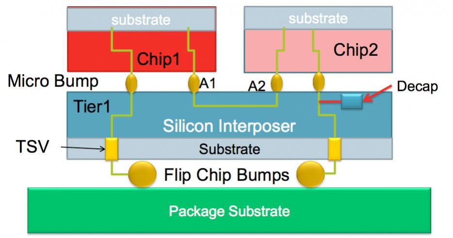 The next technique, already in production at some companies like Xilinx, is to use a silicon interposer. This is (usually) a large silicon “circuit board” with perhaps 4 layers of metal built in a non-leading edge process and also usually containing a lot of decoupling capacitors. The other die are microbumped and flipped over onto the interposer, and the interposer is connected to the package using through silicon vias (TSVs). Note that this approach does not require TSVs on the active die, avoiding a lot of complications.
I think it is several years before we will see true 3D stacks with TSVs through active die and more than two layers of silicon. It requires a lot of changes to the EDA flow, a lot of changes to the assembly flow, and the exclusion areas around TSVs (where no active circuitry can be placed) may be prohibitive, forcing the TSVs to the periphery of the die and thus lowering significantly the number of connections between die that is possible.
But all of these approaches create new problems to verify power, signal and reliability integrity. To solve this requires a new verification methodology that provides accurate modeling and simulation across the whole system: all the die, interposers, package and perhaps even the board.
TSVs and interposer design can cause inter-die noise and other reliability issues. As I said above, the interposer usually contains decaps and so the power supply integrity needs to take these into account. In fact it is not possible to analyze the die in isolation since the power distribution is on the interposer.
One approach, if all the die layout data (including the interposer) is available, is to do concurrent simulation. Typically some of the die may be from an IP or memory vendor and in this casee a mdel-based analysis can be used, with the CPMs (chip power model) standing in for the detailed data that is unavailable.
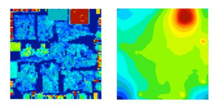 One challenge that going up in the 3rd dimension creates is the issue of thermal induced failures. Obviously heat generated has a harder time getting out from the center than in a traditional two dimensional chip design. The solution is to create a chip thermal model (CTM) for each die, that must include temperature dependent power modeling (leakage is very dependent on temperature), metal densite and self-heating power. Handing all these models to ta chip-package-system thermal/stress simulation tool for power-thermal co-analysis, the power and temperature distribution can be calculated.
A final problem is signal integrity. The wide I/O (maybe thousands of connections) between the die and the interposer can cause significant jitter due to simultaneous switching. Any SSO (simultaneously switching outputs) solution needs to consider the drivers and receivers on the different die as well as the layout of the buses on the interposer. Despite the interposer being passive (no transistors) its design still requires a comprehensive CPS methodology.
Going up into the 3rd dimension is an opportunity to get lower power, higher performance and smaller physical size (compared to multiple chips on a board). But it brings with it new verification challenges in power, thermal and signal integrity to ensure that it is all going to perform as expected.
Norman Chang’s full blog entry is here.
Related blog: TSMC Versus Intel: The Race to Semiconductors in 3D!
Share this post via:


Comments
0 Replies to “2.5D and 3D designs”
You must register or log in to view/post comments.