
 I can still remember the time, back in the mid-1980s, when I was at VLSI and we first discovered that we were going to have to worry about package pin inductance. Up until then we had been able to get away with a very simplistic model of the world since the clock rates weren’t high enough to need to worry about the package and PCB as anything other than a simple capacitive load. Put big enough transistors in the output pads and the signal would change acceptably fast. Of course, back then, 10K gates was a large chip so it was a rather simpler and more innocent time than we have today.
Those days are long gone. Now we have to analyze the chip, the package and the PCB as a single system, we can’t just orthogonally worry about the chip separately from the package and then just expect to put that package on any old PCB. In the old days, there was plenty of noise margin, we were less sensitive about trading-off increased power against reliability and there was simply less interaction between signals.
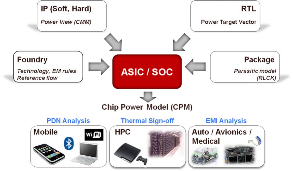
The full low-level details of the entire chip are clearly overkill for CPS analysis. Instead, a model of the die is necessary to model the noise generated by the chip. Chip power models include the die-level parasitics as well as instance switching noise. Since the model will be used for EMI emission analysis, simultaneously switching outputs (SSO) power analysis, noise analysis and more, the model must be accurate across a broad frequency range. Transistor switching noise is modeled by region-based current sources that capture the transient behavior. The power model is reduced to a SPICE format that allows long system simulations to be done using any circuit simulator.
Chip power models represent the switching noise and parasitic network of the die. The next generation of chip power model has recently become available, enabling more advanced CPS analysis methodologies. Designers are now able to probe at lower metal layer nodes in the die, to observe transistor-level noise in CPS simulation. The transient behavior of the die can now capture advanced operational modes, which are of particular interest to system engineers, such as resonance-inducing activity and transitions from low-power to high-power modes. Chip designers can now create user-configurable chip power models that can be programmed to represent different modes, depending on the simulation.
The increasing importance of CPS analysis has led Apache to create a CPS user-group to bring some standardization and interoperability to the area and create a Chip-Power Model reference flow. Besides Apache, the founding members include representatives from the top 10 semiconductor companies.
Matt Elmore’s blog on CPS
CPS user-group created by Apache


Comments
There are no comments yet.
You must register or log in to view/post comments.