The presentations from the 450mm sessions at SEMICON West are up now. After talking to equipment manufacturers and the foundries I’m fairly confident 450mm wafers will be under our Christmas trees in 2016, absolutely. TSMC just increased CAPEX again and you can be sure 450mm is part of it. SEMI has a 450mm Central landing page HERE. The SEMICON West 450mm Transition presentations are HERE. The Global 450mm Consortium is HERE. Everything you ever wanted to know about 450mm wafers just a click away; you’re welcome.
 Intel, Samsung, and TSMC have invested heavily in 450mm and will have fabs built and operational in 2015 (my opinion). Given the pricing pressures and increasing capacity demands of the mobile semiconductor market 450mm wafers will be mandatory to maintain healthy margins. Based on the data from SEMICON West and follow-up discussions, this is my quick rundown on why moving from a 12” wafer (300mm) to an 18” wafer (450mm) is the next technical innovation we will see this decade.
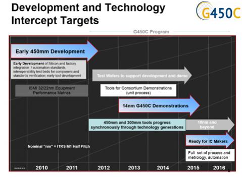
First and foremost is timing. 14nm wafers will begin production in 2014 with 10nm slated for 2016. Ramping already production worthy 14nm wafers in a new 450mm fab reduces risk and the semiconductor industry is all about reducing risk. Second is wafer margins. As I mentioned before, there will be a glut of 14nm wafers with no less than six companies (Intel, Samsung, TSMC, GLOBALFOUNDRIES, UMC, and SMIC) manufacturing them 24/7. The semiconductor industry has never ever seen this kind of total capacity increase for a given node. Add in that the mobile electronics market (phones and tablets) have reached commodity status, wafer margins will be under even more pressure than ever before. Just like the top criteria for investing in real estate: location, location, location. Wafer purchasing criteria at 20nm and below will be: price, price, price.
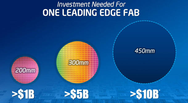
According to Intel a 450mm fab will cost twice as much as a 300mm fab with equipment accounting for the majority of the delta. The wafer handling equipment is a good example. The additional size and weight of the 450mm wafers will require complete retooling. If you have never been in a fab let me tell you it is something to see. The wafers zip around on ceiling mounted shuttles like something out of a Star Wars movie. As much as I would like to change our dinner plates at home from 12” to 18” to accommodate my increasing appetite, I certainly don’t want to buy a new dishwasher and cabinets to store them.
The ROI of 450mm wafers however is compelling. A 450mm fab with equal wafer capacity to a 300mm fab can produce 2x the amount of die. If you roughly calculate die cost, a 14nm die from a 450mm wafer will cost 23% less than a 300mm wafer. This number is an average of numbers shared with me by friends that work for: an IDM, a foundry, a large fabless company, and an equipment manufacturer. Sound reasonable?
lang: en_US


Comments
0 Replies to “450mm Wafers are Coming!”
You must register or log in to view/post comments.