

 At a lovely, but chilly, 3DIncites awards breakfast during SEMICON West, I saw Mentor Graphics win in two of five categories (Calibre 3DSTACK was the other winner). Afterwards, I talked to Steve Pateras, the product marketing director of Mentor’s test solutions about Tessent Memory BIST, which was one of the winners. I asked Pateras to explain why his memory BIST (built-in self test) tool stood out.
First some background. 3D-ICs consist of vertical stacks of bare die connected directly though the silicon. A typical 3D stack is shown in the illustration below.
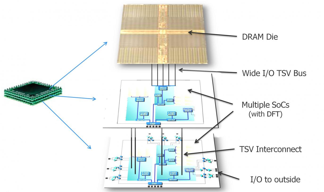
Through-silicon vias (TSVs) result in shorter and thinner connections that can be distributed across the die. TSVs reduce package size and power consumption, and increase performance.The performance boost is due to the improved physical characteristics of the very small TSV connections compared to the much larger bond wires used in traditional packaging. But TSVs complicate the test process and therefore new test solutions are critical.
Testing Memory-to-Logic Interconnect
Pateras said that applications that stack one or more memory die on top of a logic die, for example using the JEDEC Wide IO standard bus interface, are ramping quickly, so figuring out how to test the memory-to-logic configuration is a pressing concern.
The test challenge with stacked memory and logic die is testing the TSV connections. There is generally no external access to TSVs, so automatic test equipment can’t get to them without some change to the system. Functional test—like where an embedded processor is used to apply functional patterns to the memory bus—is possible but is slow, lacks test coverage, and offers little to no diagnostics.
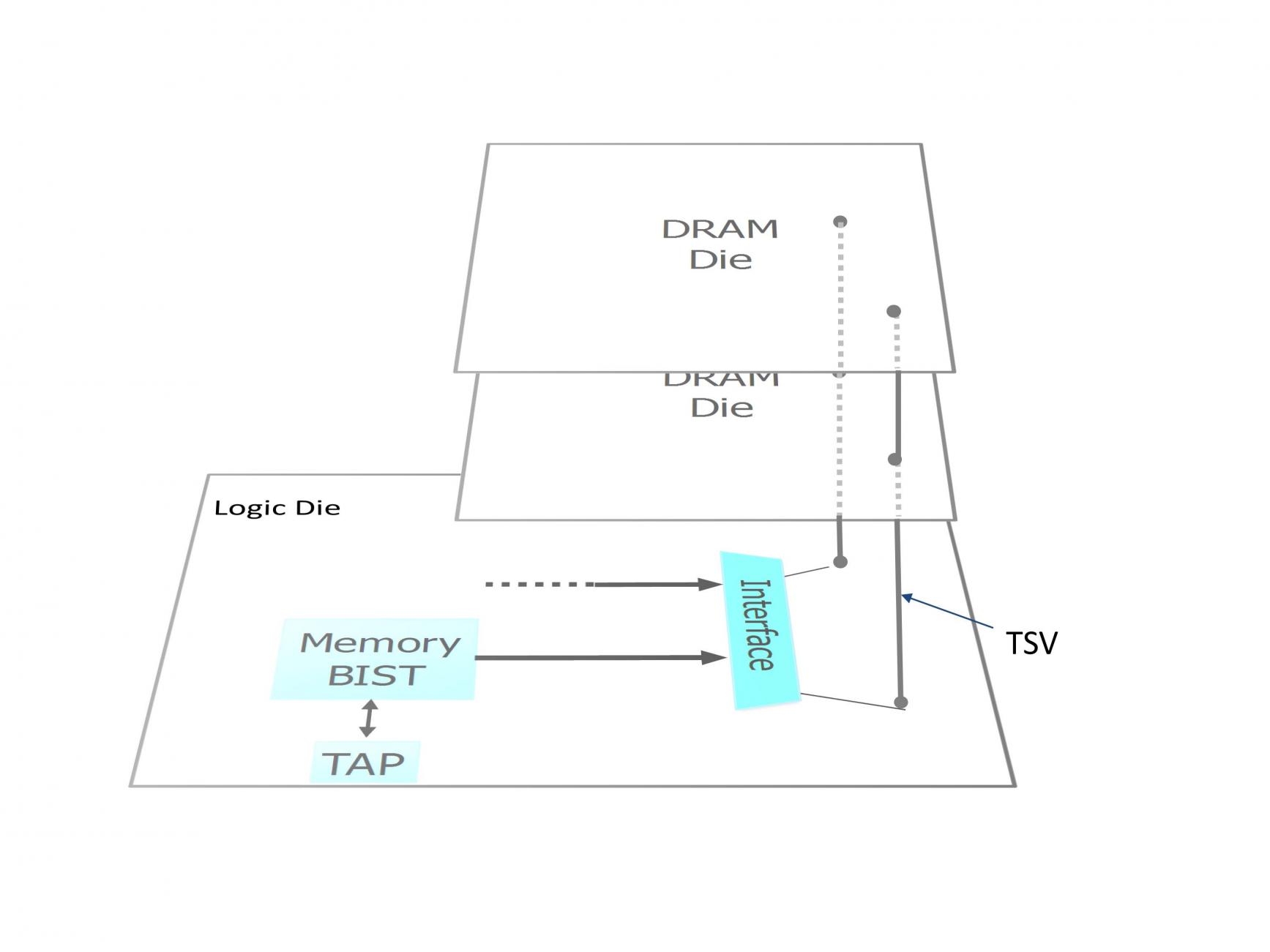
Pateras says you need an enhanced embedded test structure for test and diagnostics of memory-to-logic TSVs. Mentor Graphics’ solution is based on the BIST approach that is already commonly used to test embedded memories within SoCs. The enhancement for 3D test, says Pateras, is that the BIST engine is integrated into the logic die and communicates to the TSV-based memory bus that connects the logic die to the memory, as shown in this figure.
 Pateras says this setup provides full-speed testing of memory die and supports all popular DRAM protocols. It is flexible enough so that memory BIST controllers in a logic die can handle a variety of memory die stacked on top, which allows for different product variations without a change in test infrastructure. It also supports at-speed testing of memory buses, which covers both bond wires and TSV interconnects. Pateras calls this setup a “shared-bus capability,” and it lets you test multiple memory die on the same interconnect.
This is nifty, but why is it award-worthy? Pateras said that to make the new solution for 3D test, the Mentor engineers came up with two critical advances over existing embedded memory BIST solutions.
The first is an architecture that allows the BIST engine to communicate to a memory bus rather than directly to individual memories. This lets you test multiple stacked memories and also lets the BIST engine test the memory bus itself, and hence the TSV connections, not just the memories. He says there are test algorithms tailored to cover bus-related failures. Because of this directed testing of the memory bus, the 3D BIST engine can also report the location of failures within the bus, so you can diagnose TSV defects.
The second technical advance in this new 3D BIST solution is that it is run-time programmable. “What does that mean, Steve?” I asked, just for you, my readers.
“Well, it means that the BIST engine can be programmed in silicon for different memory counts, types, and sizes using only the standard IEEE 1149.1 JTAG test interface,” Pateras explained. Because the BIST engine is embedded into the logic die and can’t be physically modified without a design re-spin, this adaptability is essential. With full programmability, he continued, no re-design is needed over time even as different memories and memory configurations for different applications are piled on top of the logic die. And yes, Mentor has an automated flow for programming the BIST engine (for wafer or final package testing) to apply different memory test algorithms, to use different memory read/write protocols, and to test different memory bus widths and memory address ranges. You generate the patterns needed to program the engine through the JTAG interface pins in common formats, such as WGL or STIL, that can be loaded and applied by standard automatic test equipment.
I asked Pateras about the design overhead of putting this BIST in your logic die. It should have minimal impact on design flows and cost, and no impact on design performance. Pateras says an automated, standardized RTL flow will integrate the BIST engine into the logic die and verify its operation. There would be no impact to design performance, he says, because the BIST engine intercepts the memory bus with multiplexing logic placed at a point in the functional path with sufficient slack.
And this memory BIST technology is what won the 3DInCites award in the category of Test and Reliability Tools/Equipment. But it’s only part of what Mentor offers for 3D test, says Pateras.
Testing Logic-to-Logic Interconnect
Testing logic-on-logic stacks is a little different, and there are different approaches to addressing this problem. Pateras explains that in one approach, TSVs are assumed to exist between the boundaries of scan-isolated cores on neighboring die. You can then use a hierarchical ATPG capability, but instead of being on 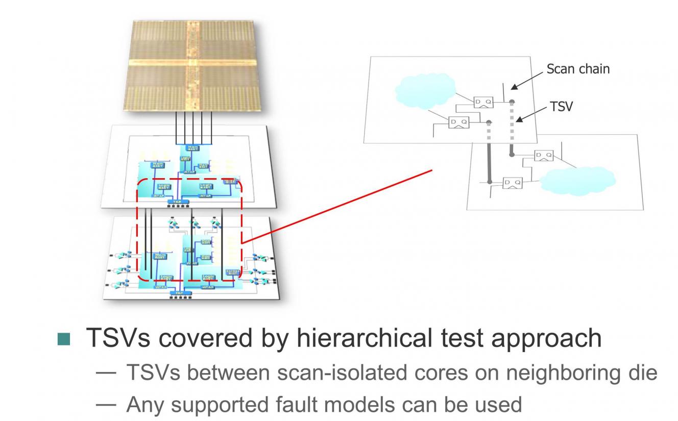 the same die, the cores involved in testing are on separate die. The test pattern generation process is essentially the same in both cases. Test patterns for the die/cores under test are generated using the full package netlist, and a gray box model is used for non-targeted die/cores.
Another approach is to place bidirectional boundary scan cells at each TSV. “The bidi cell naturally provides a wrap-around or loopback test close to the die for wafer test. In addition,” says Pateras, “the bidi supports a contactless leakage test for wafer test.”
“Whoa, Steve,” I interrupted. “Contactless leakage test is beyond the scope of this interview. I’ll come back another day for that.” There’s only so much one can absorb at a time.
“Okay, we’ll save that discussion for later,” he said. I believe he made note of it.
Back to the main topic, the boundary scan test structure and control language for scan test of stacked logic die can be modeled with IJTAG (P1687). The test patterns are then generated using standard interconnect test algorithms.
In summary, Pateras says for 3D test of stacked die and the TSVs, you need a combination of ATPG and BIST technologies, which already exist and can be deployed in any 2.5D and 3D configurations you can come up with.
For further reading, Pateras suggests Mentor’s 3D test white paper, available here (with registration): http://go.mentor.com/yqp5
Share this post via:


The Data Crisis is Unfolding – Are We Ready?