
At Semicon yesterday I attended Mentor’s presentation on improving test standards. Joe Sawicki was meant to present but he was unable to get a flight due to the ongoing disruption at SFO after last weekend’s crash. I just flew in myself and it is odd to see the carcase of that 777 just beside the runway we landed on.
The big challenges facing manufacturing test at present are:
- achieving adequate test quality
- minimizing test cost
- dealing with increased design size and resultant test complexity
- methodology and tools for testing 3D stacked die
- ramping production and yield quickly

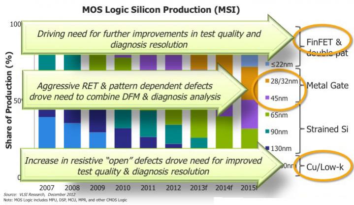
Over the last few process generations, changes in the manufacturing technology have had knock-on effects on test. First back at 180nm with damascene copper interconnect there was an increase in resistive “open” defect requiring improved test quality. Then at 45nm and below the aggressive RET decoration created pattern dependent defects requiring DFM and diagnosis to be more tightly combined. And now with FinFETs, we require further improvements in test quality and diagnosis.
Some safety critical applications such as automotive are starting to have 0 DPM (defects per million) as a quality requirement. This is obviously not appropriate for all designs: tripling the test cost for chips for cell-phones for example is the wrong trade-off. But another area requiring high test yield is for die going into any sort of 3D stack. A bad die getting through doesn’t just waste that die (and it was bad anyway), it wastes several good die and an expensive package.
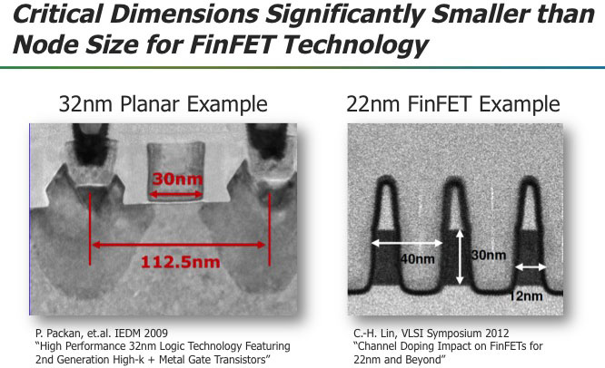
The new processes, FinFET and FD-SOI are still too new to really understand how defects will behave in new cells. But people are anticipating increased in-cell defectivity since there is a dramatic reduction in the minimum feature size for FinFETs compared to planar devices.
In the past, most test coverage has been based on stuck-at fault models. This assumes that a test is good if it detects whether the output of a cell that is stuck at 0 or stuck at 1 causes the test to fail. Everyone knows that this is not really a realistic model of all ways that chips actually fail but it has been surprisingly robust and it is easy to measure.
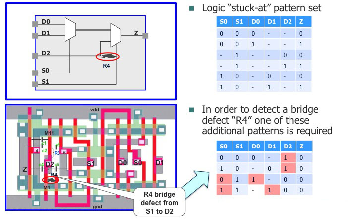
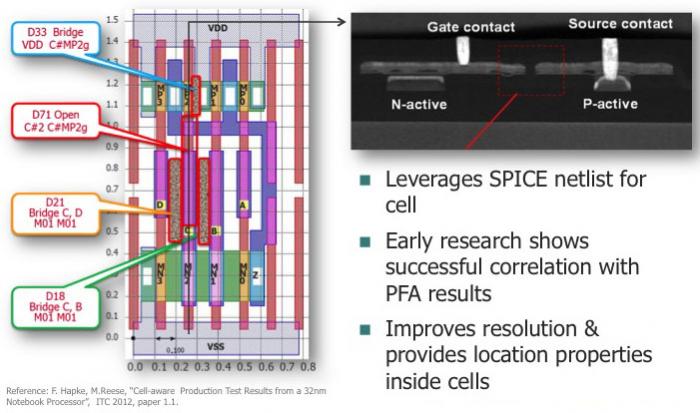
But with more complex processes (and RET and more complex failure modes) this is not enough. The first thing to do is to look inside the cells and use cell-aware ATPG to look for undetected faults based on the actual cell layout and transistor netlist structure. One particular problem with FinFETs is strength related defects. Since transistors are a fixed size and multiple fins are used for higher drive, there is the risk that not all the transistors fail and so the drive will not be adequate but the circuit will still be functionally correct.
AMD did some work with Mentor on improving quality using cell-aware ATPG. Compared to just using the regular stuck-at model, they improved test quality at wafer sort by an incredible 885 DPM. This is a huge number. It was high enough to hugely reduce the need for system level functional test.
The next issue is to be able to drill down into systematic failures, where many more chips than expected fail on the same vector. The fix, for example, may be to redo the DFM decoration to improve yield, but that requires the capability to look for pattern-related failures and to isolate the problem not just to a net but to the correct segment of the net.
So in the new era there will be changes in test methodology:
- need better detection of FinFET defect mechanisms (within the cells)
- need further improvements in diagnosis resolution and root-cause determination
Obviously with its strong position in test, Mentor plans to deliver the required capabilities in the future.
LATE NEWS: at 1pm today at Sematech Mentor’s TestKompress with cell-aware ATPG was awarded the Best of West award. The award recognizes important product and technology developments in the microelectronics supply chain. The Best of West finalists were selected based on their financial impact on the industry, engineering or scientific achievement, and/or societal impact.


The Data Crisis is Unfolding – Are We Ready?