
Last week Berkeley Design Automation introduced a new Analog Characterization Environment (ACE) – a high-productivity system to ensure analog circuits meet all specifications under all expected operational, environmental, and process conditions prior to tapeout.
While standard cell characterization and memory characterization are well defined application areas with standard flows, dedicated tooling, and rigorous metrics to ensure high quality results, analog circuit characterization is still largely ad hoc and highly dependent on individual designers’ experience. As a result analog circuit results in silicon are predictably unpredictable. Berkeley Design Automation has set out to change that with ACE.
Two Analog Worlds
Understanding the need for ACE requires first understanding the current environment analog designers work within. For leading-edge analog circuit design and verification, there are two separate and distinct worlds today:
Analog World 1 – The High-Performance Analog/Mixed-Signal World: In this world ICs are dominated by precision analog/RF circuitry including: sensors, ADCs, DACs, PLLs, RF, filters, power management, etc., and integrated digital is important and growing. Cadence dominates World 1, and Synopsys is rarely seen. Cadence simulators (Spectre, Spectre Turbo, Spectre RF, APS, APS RF, UltraSim, etc.) have historically dominated World 1, but BDA Analog FastSPICE (AFS) has made significant inroads handling the toughest problems in the last few years. All World 1 simulators use Spectre syntax and models. World 1 lives within Cadence ADE 5.1 or ADE-L/ADE-XL 6.1. World 1 designers wouldn’t dream of manually editing a netlist or doing anything from the command line.
Analog World 2 – The Big-Digital SoC World: With all due respect to digital design teams, SoC performance bottlenecks are all analog: i) high-speed I/O (getting data on and off the chip), ii) PLL/clocking (any slop in the clock is a tax on every digital path), and iii) memory (half the silicon area). Synopsys dominates World 2, and Cadence is rarely seen. Synopsys simulators (HSPICE, HSIM, NanoSim, XA, FineSim) have historically dominated World 2, but again BDA AFS has made significant inroads handling the toughest problems in the last few years. All World 2 simulators use HSPICE syntax and models. World 2 lives at the command-line—manually editing netlists, scripting, and issuing command-line runs. World 2 designers wouldn’t dream of doing anything through Cadence ADE.
BDA uniquely competes very effectively in both of these worlds, giving it a unique viewpoint on the market. Moreover, increasingly World 1 is meeting World 2 on the same project, making analog characterization an even bigger challenge.
The Growing Need for Analog Characterization
Analog designers’ simulation tasks may be classified as performance verification (hereafter simply “verification”) followed by characterization. As used here, verification is what designers do to make sure their circuit meets specifications under nominal conditions and under a few conditions that the designer expects may break it – perhaps a few PVT corners, a few extreme operating conditions, and maybe a bit of Monte Carlo for mismatch. Everything looks good. Verification is done. The circuit is probably good to go, and the designer would like to move on to the next interesting problem.
Not so fast. There are many possible process, voltage, and temperature corners in nanometer silicon technologies. There are many possible operating conditions (e.g., signal levels, calibration setups, operating modes, and noise sources). There is also a lot of global and local process variation. The process corners in the PDK do not correspond to any analog circuit’s 3-sigma points. In fact, often they are not even close. Global process variation affects every circuit and every measurement (e.g., frequency, gain, duty cycle, jitter, SNDR, etc.) in every circuit differently. Key design components (e.g., inductors, varactors, etc) also have critical variation. What combination of these different environmental, operational, and process conditions (a.k.a., “variants”) result in a blown spec in silicon is anyone’s guess—especially since today’s circuits are almost all highly nonlinear. This is a combinatorial problem with typically 100s or 1000s of known important variants. The objective of analog characterization is to ensure an analog/mixed-signal/RF circuit meets all specs under all these variants.
Characterization is not fun. It’s tedious, it’s boring, it’s error-prone, it takes a long time…and there haven’t been any good tools to help. As a result, analog designers cut corners—a lot of corners (and sweeps and Monte Carlo runs). Although designers know they should do a lot more characterization, it is too painful and takes too long. So they don’t. Instead they make sure their circuits have plenty of margin (no one’s measuring over-design anyway) and hope that they don’t miss a scenario that causes a silicon problem.
Characterization in the Two Analog Worlds
In World 1 designers live within ADE. By all accounts ADE is pretty good for verification setup and analysis, but it is not so good for characterization. All Cadence customers are migrating to ADE 6.1, in which most characterization capabilities are in ADE-XL. Many designers find ADE-XL so cumbersome that they are actually performing less characterization than before. For example, setting up a corner is completely different than setting up a sweep and both are completely different than setting up a Monte Carlo. Non-trivial combinations of corners, sweeps, and Monte Carlo require OCEAN scripting for setup and post-processing. After a characterization run, designers find it impractical to effectively mine their own data, let alone look at results across a project.
In World 2 designers hand-edit netlists and write scripts. Many of the simulators, including HSPICE, have very limited support for combinations of corners, sweeps, and Monte Carlo making it very difficult to setup some of the most obvious combinations (e.g., a temperature sweep under a voltage sweep). In this world every designer does things differently, so it’s impractical to mine characterization data in any consistent way.
ACE and Beyond
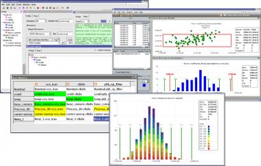
Analog characterization is not rocket science. It requires straightforward tool design and engineering—analytics for analog. It didn’t exist, so BDA developed the Analog Characterization Environment. ACE is an environment where basic units like tests, measurements, and variants (i.e., corners, sweeps, and Monte Carlo runs) are characterization building blocks that are easy to create, easy to combine, and easy to reuse. ACE makes it easy to specify the experiments you want to run. ACE makes it easy to view the results and analyze the data. ACE makes it easy to create regressions. ACE makes it easy for designers, CAD engineers, and third parties to access, use, and add to the characterization data.
ACE makes systematic analog characterization practical, but it is only the first step. BDA created ACE with true openness in mind. ACE stores all characterization data in an Open Verification Database (OVD) that is quite literally open to all. All OVD data is in standard formats wherever applicable and where standard formats don’t exist, the data is in XML if intended for tools or text if intended for designers. OVD provides a foundation for CAD engineers, designers, and third-parties to integrate analog characterization into the rest of their IC design process from top-down specification and digital verification to configuration management, variation analysis, and circuit optimization tools (e.g., Cadence, MunEDA, and Solido). BDA is already working on a number of extensions and encourages customers and third-parties to do likewise.
Visit BDA at #50DAC and see Analog Characterization Environment!
lang: en_US


Real men have fabs!