
FinFETs are fun! They certainly have kept me busy writing over the past year about the possibilities and probabilities of a disruptive technology that will dramatically change the semiconductor ecosystem. Now that 14nm silicon is making the rounds I will be able to start writing about the realities of FinFETs which is very exciting!

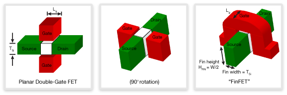
From Moore’s Law, we can infer that FinFETs represent the most radical shift in semiconductor technology in over 40 years. When Gordon Moore came up with his “law” back in 1965, he had in mind a design of about 50 components. Today’s chips consist of billions of transistors and design teams strive for “better, sooner, cheaper” products with every new process node. However, as feature sizes have become finer, the perils of high leakage current due to short-channel effects and varying dopant levels have threatened to derail the industry’s progress to smaller geometries.
Synopsys published an article FinFET: The Promises and the Challenges which is a very good primer and talks about the FinFET Promise:
Leading foundries estimate the additional processing cost of 3D devices to be 2% to 5% higher than that of the corresponding Planar wafer fabrication. FinFETs are estimated to be up to 37% faster while using less than half the dynamic power or cut static leakage current by as much as 90%.
The foundries, on purpose or by accident, made the right decision in taking the 20nm planar process and adding FinFETs. Ramping a new process and a new 3D transistor would have been daunting for the SoC based fabless semiconductor ecosystem. Even for Intel, they may have 22nm Tri-Gate microprocessors but I have yet to see a 3D SoC from them. FinFET Design enablement (EDA and IP) is a big part of that transition and I have to give Synopsys the advantage here.
The foundry’s intent is to ensure the transition to FinFET is as transparent as possible, allowing users to seamlessly scale designs to increasingly smaller geometry processes. Maximum benefits with this technology will require implementation tools to minimize power consumption and maximize utilization and clock speed. FinFETs require some specific enhancements made in the following areas: TCAD Tools, Mask Synthesis, Transistor Models, SPICE Simulation Tools, RC Extraction Tools and Physical Verification Tools.
Synopsys building critical IP mass over the years, especially buying Virage Logic, has given them an early and intimate look at the bleeding edge of process development. Yes I have seen fluffy 14nm test chip press releases from all vendors but the foundation IP (SRAM) is where the rubber first meets the road and that gives Synopsys a lead on tool development.
That is why I asked Raymond Leung, VP of SRAM development at Synopsys, to present at the EDPS Conference FinFET Day that I’m keynoting. Not only does Raymond have deep SRAM experience from Virage, he also led SRAM development at UMC. At Synopsys, Raymond now gets first silicon at the new processes nodes at ALL of the foundries, so his presentation on FinFET design challenges will be something you won’t want to miss!
Don’t forget to log into the webinar I’m moderating on Unlocking the Full Potential of Soft IP with Atrenta, TSMC, and Sonics Tuesday, March 5, 2013 9 a.m. Pacific Time. You just never know what I’m going to say so be sure and catch the live uncensored version!


Comments
0 Replies to “Synopsys ♥ FinFETs”
You must register or log in to view/post comments.