

My oldest son just upgraded Smart Phones from a 3″ display to a 4.5″ display and was shocked to discover that his battery barely lasted 8 hours, so I welcomed him to the reality of limited battery life in modern SoC-based mobile devices. There is some hope in increasing battery life for our consumer-oriented devices and the engineers at Cadence make a case for this in a White Paper: Building Energy-Efficient ICs from the Ground Up.

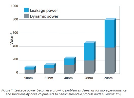
The effects of leakage power have dramatically increased as IC process nodes have migrated from 65nm down to 20nm as shown in the following chart from IBS:
Even when you can use innovative design or process techniques to reduce power consumption, there’s another issue with modern SoCs – heat dissipation. With millions of active MOS devices on a single chip the heat created by the chip starts to:
- Decrease the reliability of the device
- Shortens the battery life
- Requires cooling fans or heat spreaders which increase product cost
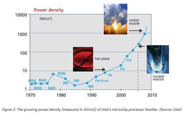
Just a few years ago the microprocessors from Intel were on a power trajectory that was unsustainable:
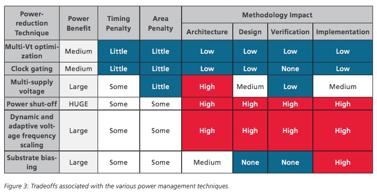
Engineers now have a range of techniques to control chip and system-level power, like:
- Multi-Vt transistors where non-critical paths can use higher Vt transistors to lower leakage and switching power.
- Multiple-supply Voltage (MSV) – using voltage islands for functional blocks to further control the performance, so that lower performance blocks can use a lower supply voltage, conserving power. Higher-performance blocks can use a higher voltage to get better speed.
- Power shutoff (PSO) – a functional block can be shut down when not required. Further decisions include when to retain state of the functional block or not.
- Standby mode – a functional block can have it’s supply reduced low enough that it retains state, but is not logically functioning.
- Substrate biasing – the substrate can have a voltage applied that in turn effects the Vt of all devices, controlling the speed and power required.
- Dynamic voltage and frequency scaling (DVFS) – while the SoC is running a functional block may have its supply or frequency boosted to get temporary performance, then reduced to conserve power.
- Adaptive voltage scaling (AVS) – an on-chip process and temperature monitor decides what voltage level to use.
- Clock gating – the RTL can be modified to effectively shut off clock toggling to a functional block when that block isn’t producing active results.
Multiple techniques can be used together in managing power:
Common Power Format
Cadence and other vendors have created a specification called the Common Power Format, now under the control of the Si2 Low Power Coalition. With the CPF approach your design team can capture power-aware design intent, specify constraints, and use automation techniques to achieve your power budget.
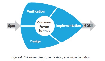
Your flow with CPF will follow:
- Chip Planning – at the architectural specification making early trade-offs. Uses the Cadence InCyte Chip Estimator tool.
- Power Analysis – includes running power analysis throughout the design process, down to implementation steps.
- Top-Down Multi-Objective Optimization – having logic and physical synthesis work together at the same time to optimize for power, area and timing.
- Verification – both simulation-based and static formal verification are used to verify a design against objectives. Cadence tools are the Incisive Enterprise Simulator, Palladium and Encounter Conformal.
- Power-Aware Test – DFT techniques are assembled for logic BIST, memory BIST, ATPG and compression. The flow has to be power-aware to meet your specs.
- Physical Design – implementation includes RTL synthesis, silicon virtual prototyping, floorplan synthesis, clock tree synthesis, DFM, DFY, and P&R. The Encounter Digital Implementation System is used.
- Power Grid – part of the P&R is to create power domains that are planned and meet specifications for Voltage IR drops, ground bounce on VSS, and Electro-Migration (EM).
- Power Rail – The power distribution network (PDN) includes the SoC and the packaging, so the entire system needs to be analyzed.
- Signal Integrity – SI analysis will look at how nets toggle and impact adjacent nets through capacitive coupling.
- Signoff – the final series of checks to verify that the power budget has been met with a power grid that is design just right, not over or under-designed.
Conclusion
It takes an industry working together to create design and fabrication techniques that will meet the power challenges of modern, hand-held devices that need to run all day long between battery charges. The Common Power Format was released back in 2007 and has since been used as an approach on thousands of low-power designs.
A similar but competing approach dubbed Unified Power Format (UPF) was proposed by Synopsys and Mentor Graphics.
Share this post via:


Comments
0 Replies to “Building Energy-Efficient ICs from the Ground Up”
You must register or log in to view/post comments.