The concept of Non Volatile Memory (NVM) block which could be integrated into an ASIC is relatively recent, Novocell for example has been created in 2001. NVM IP integration into an ASIC is a pretty smart technology: integrating from a few bytes to up to Mbits into a SoC can help reducing the number of chips in a system, increase security and allow for Digital Right Management (DRM) for video and TV applications, or provides encryption capability.
In the past (in the 1990’s) integrating a Flash memory block into a SoC was requesting to add specific mask levels, leading to an over-cost of about 40%. I remember trying to sell such an ASIC solution in 1999-2001: the Flash memory capability was looking very attractive for the customer, until we talk about pricing and the customer realizes that the entire chip would be impacted. I made few, very, very few sales of ASIC with embedded Flash! The current NVM IP offering from Novocell Semiconductor does not generate such a cost penalty; the blocks can be embedded in standard Logic CMOS without any additional process or post process steps and can be programmed at the wafer level, in package, or in the field, as en use requires.
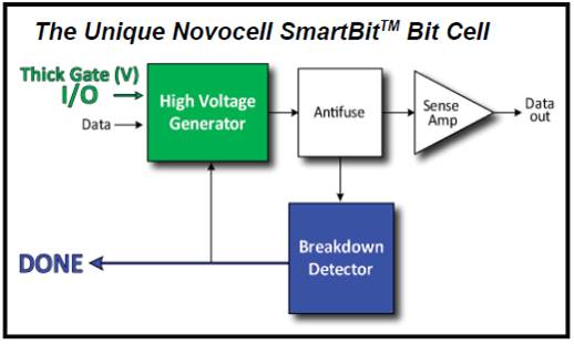
An interesting feature offered by the Novocell NVM family, based on antifuse One Time Programmable (OTP) technology, is the “breakdown detector”. Does that means that, if you do not use this function, delivered only by Novocell, you may program an OTP, by activating the antifuse, and finally getting an apparently programmed memory cell, or if you prefer, a memory cell which you think you have programmed, but in fact that the cell is NOT containing the desired value? The answer is, unfortunately for Novocell competitors, YES!
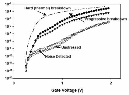
The breakdown detector is used to precisely determining when the voltage applied to the gate (breaking the oxide and consequently allowing the current to flow through this oxide, and finally programming the memory cell) will effectively have created an irreversible oxide breakdown, the “hard breakdown”, by opposition of a “soft breakdown” which is an apparent, reversible oxide breakdown. If, for example, the oxide has been stressed during a period of time which is not long enough, the hard breakdown is not effective and the user can’t program the memory cell. Looking at the two pictures help understanding the mechanisms:
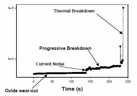
- On the first, the current (vs time) is going up sharply only after the thermal breakdown is effective
- The next pictures shows the current behavior of a memory cell for different cases, and we can see that when the hard breakdown is effective the current value is about three order of magnitude higher than for a progressive (or soft) breakdown.
When your NVM IP does not include a breakdown detector, you can find some way to increase your level of confidence into the OTP programming; we will see two of these:
- You can choose to increase the time duration during which you apply this high voltage. But you have to know that such a time is strongly dependent on technology factors, like oxide thickness, doping concentration of the substrate, and so on. This time duration varies between different technologies nodes, this seems quite obvious, but it also varies, for the same technology node, with the Silicon foundry selected. So, you can say you will multiply the average time by a factor of 2. Or maybe you should multiply by a factor of 5? Or 10? In other word, if you plan to program a large OTP, you will consume more than needed tester time, which is, as everybody knows, very cheap!
- If you use the above mentioned approach, you have to keep in mind that, whatever the time duration selected, there is a (statistically) remaining risk that “some” cell may not have been properly programmed. Thus, NVM IP vendors (these who are not using the “breakdown detector”) have decided to add spare memory points. In fact, they have quickly realized that to be sure to have enough margin, they should duplicate the memory array! The cost in term of wasted silicon area is proportional with the memory size…
Clearly, one of the Novocell’s differentiator, and probably the most important, is reliability. To avoid the limitations of traditional embedded NVM technology, Novocell utilizes the patented dynamic programming and monitoring process and method of the Novocell SmartBit™, ensuring that 100% of customers’ embedded bit cells are fully programmed. The result is Novocell’s unmatched 100% yield and unparalleled reliability, guaranteeing customers that their data is fully programmed initially, and will remain so for an industry leading 30 years or more. Novocell NVM IP scales to meet all NVM size and complexity challenges that grow exponentially as SoCs continue to move to advanced nodes such as 45nm and beyond.
Eric Estevefrom IPNEST
A Brief History of Semiconductor IP


The Data Crisis is Unfolding – Are We Ready?