

Mark Twain remarked that everyone talks about the weather but nobody does anything about it. 3D ICs seems to be a bit like that. Over the last couple of years there have been lots of people talking about 3D but very little that has actually been manufactured. In addition to the weather, everyone talks about Xilinx’s 3D Virtex design because it is about the only one that is in manufacturing (it is so high end I hesitate to say it is “volume manufacturing”).
All of Cadence, Synopsys and Mentor have talked about some aspects of 3D in their toolsets. The challenge with 3D is that it affects everything from synthesis on down and if only a few tools have been updated it is like a ladder with missing rungs, hard to get from one end to the other of the design flow.
At DAC, Cadence announced a full suite of tools that they have been working on with TSMC to create what they are calling the CoWoS Design Ecosystem. I met with John Murphy and Samta Bansal to find out more. The first obvious question is CoWoS, what is that? It stands for chip-on-wafer-on-substrate (or sometimes on-silicon) and is TSMC’s name for their heterogeneous silicon interposer approach. Heterogeneous in the sense that all the die on the interposer do not need to be from the same semiconductor process.
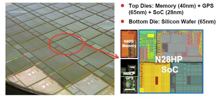 As a test vehicle the designed and manufactured the first heterogeneous CoWoS module. There were 3 die: a 40nm memory, a 65nm GPS and a 28nm SoC, all put together on a 65nm silicon wafer. And it is yielding. Nobody is saying how much yet, but just as with the Xilinx part, one of the major reasons for doing this sort of design is to get the learning experience of what it takes to make an economic solution.
As a result there is now a path for 2.5D interposer-based technology through a Cadence (almost entirely) flow from implementation, to analysis, to verification and including DFT and test solutions.
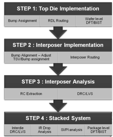 The flow starts with a fairly standard implementation of the top die, obviously bumped rather than designed to be bonded out, but using standard RDL routing. Wafer test is developed (which is very important in 3D designs, lots of known-good-die get wasted when a bad die slips through wafer sort). Next the interposer is designed and routed. The interposer itself needs to be analyzed and then the whole system of interposer and die (and I’m guessing package) to check everything is correct, that IR drop is within tolerance and pulling all the test together for a package level test that can test everything
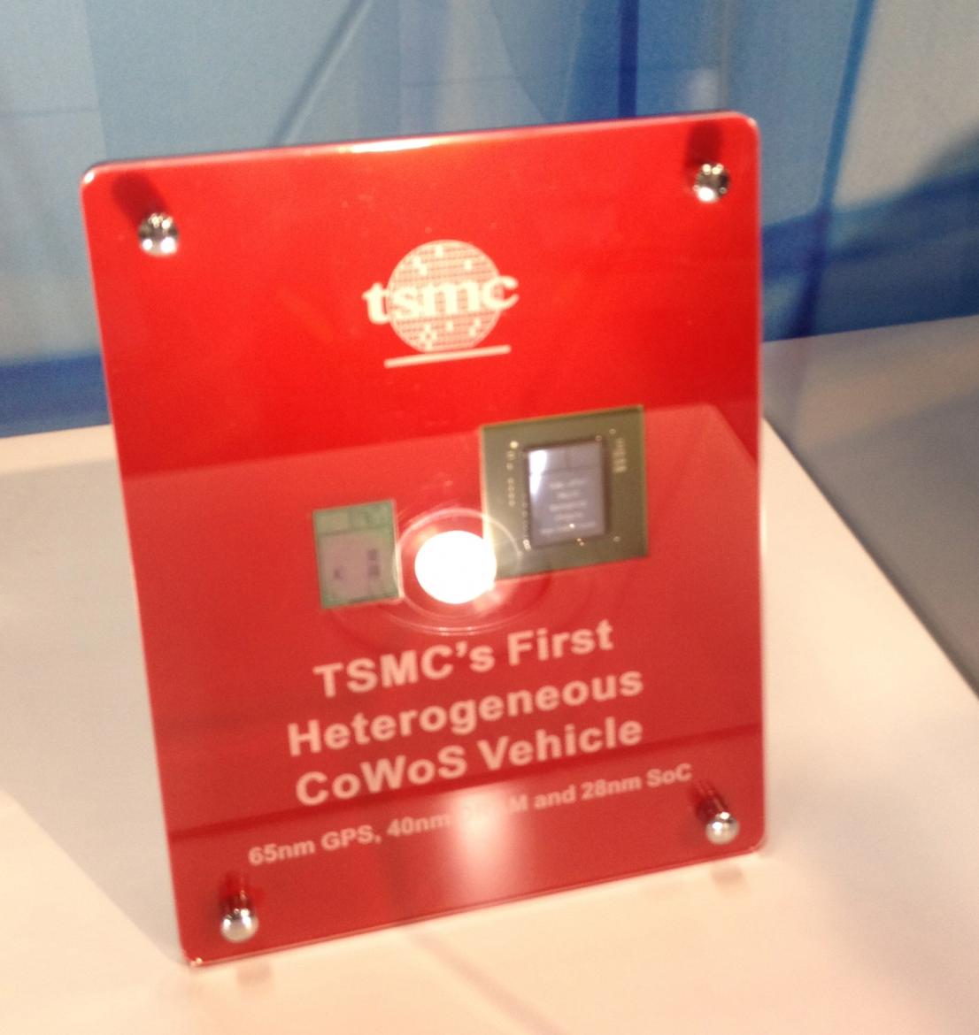 Above is the first module on the Cadence booth. They also had it on the TSMC booth — but with big signs saying no cameras or camera-phones. I think this probably just reflects different cultural attitudes to secrecy. Cadence has done several other 2.5D chips. Nobody is yet ready to announced but Cadence claim 8 testchips and 1 production chip.


Comments
There are no comments yet.
You must register or log in to view/post comments.